ZHCSN08D August 2020 – April 2024 DRV8714-Q1 , DRV8718-Q1
PRODMIX
- 1
- 1 特性
- 2 应用
- 3 说明
- 4 Device Comparison Table
- 5 Pin Configuration and Functions
- 6 Specifications
-
7 Detailed Description
- 7.1 Overview
- 7.2 Functional Block Diagram
- 7.3
Feature Description
- 7.3.1 External Components
- 7.3.2 Device Interface Variants
- 7.3.3 Input PWM Control Modes
- 7.3.4 Smart Gate Driver
- 7.3.5 Tripler (Dual-Stage) Charge Pump
- 7.3.6 Wide Common-Mode Current Shunt Amplifiers
- 7.3.7 Pin Diagrams
- 7.3.8
Protection and Diagnostics
- 7.3.8.1 Gate Driver Disable (DRVOFF/nFLT and EN_DRV)
- 7.3.8.2 Low IQ Powered Off Braking (POB, BRAKE)
- 7.3.8.3 Fault Reset (CLR_FLT)
- 7.3.8.4 DVDD Logic Supply Power on Reset (DVDD_POR)
- 7.3.8.5 PVDD Supply Undervoltage Monitor (PVDD_UV)
- 7.3.8.6 PVDD Supply Overvoltage Monitor (PVDD_OV)
- 7.3.8.7 VCP Charge Pump Undervoltage Lockout (VCP_UV)
- 7.3.8.8 MOSFET VDS Overcurrent Protection (VDS_OCP)
- 7.3.8.9 Gate Driver Fault (VGS_GDF)
- 7.3.8.10 Thermal Warning (OTW)
- 7.3.8.11 Thermal Shutdown (OTSD)
- 7.3.8.12 Offline Short Circuit and Open Load Detection (OOL and OSC)
- 7.3.8.13 Watchdog Timer
- 7.3.8.14 Fault Detection and Response Summary Table
- 7.4 Device Functional Modes
- 7.5 Programming
- 8 Register Maps
- 9 Application Implementation
- 10Device Documentation and Support
- 11Revision History
- 12Mechanical, Packaging, and Orderable Information
7.3.8.2 Low IQ Powered Off Braking (POB, BRAKE)
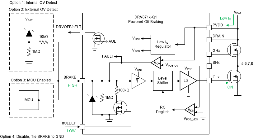
The DRV871x-Q1 provide the ability to enable the low-side gate drivers while the device is in its low-power sleep mode (nSLEEP = logic low). This allows the external low-side power MOSFETs to be enabled while maintaining a low quiescent current draw from the power supply. Enabling the external low-side MOSFETs allows the device to actively brake a motor connected to the external half-bridges by shorting the back emf across the motor terminals. This can help prevent reverse driving of the motor by an external force from overcharging the system power supply by dissipating the energy in the low-side MOSFETs. This function is only available while the device is in its low-power sleep mode. The function is enabled by taking the BRAKE pin to logic high.
The powered off braking function is available on half-bridges 5, 6, 7, and 8 on the DRV8718-Q1 device. On the DRV8714-Q1, the power off braking function is available on all four half-bridges. The BRAKE pin will enable or disable the low-side gate drivers for all four of the half-bridges together. The powered off braking function requires the PVDD voltage supply to be present in order to enable the low-side gate drivers, but the function can operate without the DVDD logic power supply present.
In case of a short circuit to power supply fault present on the power stage, a simple overcurrent detector circuit with analog RC deglitch filter is provided to disable the low-side MOSFET if a high current event is detected while braking. This is needed since the normal overcurrent protection circuits are disabled during the device low-power sleep mode. The overcurrent comparator and RC deglitch filter values are fixed and cannot be adjusted.
The powered off braking function is enabled through the BRAKE pin and the BRAKE pin can be pulled high through several different methods. To reduce quiescent current draw, the pulldown resistance of the BRAKE pin is reduced to 1MOhm while in device low-power sleep mode. The BRAKE pin can be always left high while the device is in low-power sleep mode or can be set high in response to a rising voltage on the power supply. The BRAKE pin has an internal voltage clamp allowing it to be connected directly to the PVDD battery supply through a Zener diode (to set overvoltage threshold) with a series resistor to limit the current. The powered off function can be set to automatically enable in low-power sleep mode by leaving the BRAKE pin disconnected and relying on the internal overvoltage monitor.
Some methods to pull up the BRAKE pin and enable the powered off braking function include:
- Option 1: Internal overvoltage monitor. BRAKE pin should be left not-connected (Hi-Z)
- Option 2: Voltage triggered pull up with passive Zener diode. An external Zener diode can be added to the BRAKE pin to create an overvoltage trigger that is lower than the internal overvoltage monitor.
- Option 3: MCU fixed digital output high or MCU digital output in response to motor movement detected by senor or rising voltage. A digital output to the BRAKE pin can directly control whether the power off braking function is enabled (LO = disabled, HI = enabled).
- Option 4: The power off braking function can be disabled by shorting/connecting the BRAKE pin directly to PCB ground.
By default (BRAKE pin not connected), the powered off braking function is enabled by an internal overvoltage monitor that will detect the PVDD voltage and enable the low-side braking if voltage crosses the comparator threshold. The internal overvoltage monitor and power off braking function can be disabled by shorting the BRAKE pin directly to PCB ground.
 Figure 7-28 Powered Off Braking
If the powered off braking function is not utilized, the BRAKE pin should be connected directly to GND.