ZHCSQ96 July 2021 DRV8770
PRODUCTION DATA
- 1 特性
- 2 应用
- 3 说明
- 4 Revision History
- 5 Pin Configuration and Functions
- 6 Specifications
- 7 Detailed Description
- 8 Application and Implementation
- 9 Power Supply Recommendations
- 10Layout
- 11Device and Documentation Support
- 12Mechanical, Packaging, and Orderable Information
封装选项
请参考 PDF 数据表获取器件具体的封装图。
机械数据 (封装 | 引脚)
- RGE|24
散热焊盘机械数据 (封装 | 引脚)
- RGE|24
订购信息
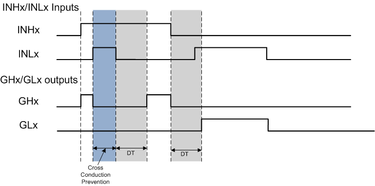
7.3.1.1.2 Deadtime and Cross-Conduction Prevention
In the DRV8770, high- and low-side inputs operate independently, with an exception to prevent cross conduction when high and low side are turned ON at same time. The DRV8770 turns OFF high- and low- side output to prevent shoot through when high- and low-side inputs are logic high at same time.
The DRV8770 also provides deadtime insertion to prevents both external MOSFETs of each power-stage from switching on at the same time. In devices with DT pin (QFN package device), deadtime can be linearily adjusted between 200 ns to 2000 ns by connecting resistor between DT and ground. When DT pin is connected to ground, fixed deadtime of 200 ns (typical value) is inserted. The value of resistor can be caculated using Equation 1.

In device without DT pin (TSSOP package device), fixed deadtime of 200 ns (Typical value) is inserted to prevent high and low side gate output turning on at same time.
 Figure 7-2 Cross Conduction Prevention
and Deadtime Insertion