ZHCSNT9K July   2008  – March 2021 DRV8800 , DRV8801

PRODUCTION DATA  

  1. 特性
  2. 应用
  3. 说明
  4. Revision History
  5. Pin Configuration and Functions
  6. Specifications
    1. 6.1 Absolute Maximum Ratings
    2. 6.2 ESD Ratings
    3. 6.3 Recommended Operating Conditions
    4. 6.4 Thermal Information
    5. 6.5 Electrical Characteristics
    6. 6.6 Typical Characteristics
  7. Parameter Measurement Information
  8. Detailed Description
    1. 8.1 Overview
    2. 8.2 Functional Block Diagrams
    3. 8.3 Feature Description
      1. 8.3.1  Logic Inputs
      2. 8.3.2  VREG (DRV8800 Only)
      3. 8.3.3  VPROPI (DRV8801 Only)
        1. 8.3.3.1 Connecting VPROPI Output to ADC
      4. 8.3.4  Charge Pump
      5. 8.3.5  Shutdown
      6. 8.3.6  Low-Power Mode
      7. 8.3.7  Braking
      8. 8.3.8  Diagnostic Output
      9. 8.3.9  Thermal Shutdown (TSD)
      10. 8.3.10 Overcurrent Protection
      11. 8.3.11 SENSE
    4. 8.4 Device Functional Modes
      1. 8.4.1 Device Operation
        1. 8.4.1.1 Slow-Decay SR (Brake Mode)
        2. 8.4.1.2 Fast Decay With Synchronous Rectification
          1. 8.4.1.2.1 34
  9. Application and Implementation
    1. 9.1 Application Information
    2. 9.2 Typical Application
      1. 9.2.1 Design Requirements
      2. 9.2.2 Detailed Design Procedure
        1. 9.2.2.1 Motor Voltage
        2. 9.2.2.2 Power Dissipation
        3. 9.2.2.3 Thermal Considerations
          1. 9.2.2.3.1 Junction-to-Ambiant Thermal Impedance (ƟJA)
        4. 9.2.2.4 Motor Current Trip Point
        5. 9.2.2.5 Sense Resistor Selection
        6. 9.2.2.6 Drive Current
      3. 9.2.3 Pulse-Width Modulating
        1. 9.2.3.1 Pulse-Width Modulating ENABLE
        2. 9.2.3.2 Pulse-Width Modulating PHASE
      4. 9.2.4 Application Curves
    3. 9.3 Parallel Configuration
      1. 9.3.1 Parallel Connections
      2. 9.3.2 Non – Parallel Connections
      3. 9.3.3 Wiring nFAULT as Wired OR
      4. 9.3.4 Electrical Considerations
        1. 9.3.4.1 Device Spacing
        2. 9.3.4.2 Recirculation Current Handling
        3. 9.3.4.3 Sense Resistor Selection
        4. 9.3.4.4 Maximum System Current
  10. 10Power Supply Recommendations
    1. 10.1 Bulk Capacitance
  11. 11Layout
    1. 11.1 Layout Guidelines
    2. 11.2 Layout Example
  12. 12Device and Documentation Support
    1. 12.1 Related Links
    2. 12.2 Trademarks
    3. 12.3 静电放电警告
    4. 12.4 术语表
  13. 13Mechanical, Packaging, and Orderable Information

封装选项

机械数据 (封装 | 引脚)
散热焊盘机械数据 (封装 | 引脚)
订购信息

Recirculation Current Handling

During recirculation, it is not possible to synchronize all devices connected in parallel so that the current is equally distributed. Also, during the asynchronous portion of the current decay, the body diode with the lowest forward voltage will start conducting and sink all of the current. Said body diode is not meant to handle the new increased current capacity and will be severely affected if allowed to sink current of said magnitude.

In order to assure proper operation when devices are connected in parallel, it is imperative that external schottky diodes be used. These schottky diodes will conduct during the asynchronous portion of the recirculation mode and will sink the inductive load current until the respective FET switches are brought online.

Schottky diodes should be connected as shown in #FIG_XY4_XPC_SNB.
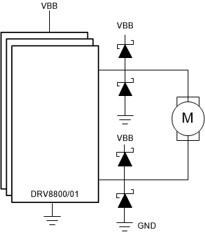
GUID-20201117-CA0I-T2V3-QVLS-4XNZPDCMVDKC-low.gif Figure 9-10 Schottky Diodes Connection