ZHCS091D February 2011 – March 2021 DRV8801-Q1
PRODUCTION DATA
- 1 特性
- 2 应用
- 3 说明
- 4 Revision History
- 5 Pin Configuration and Functions
- 6 Specifications
-
7 Detailed Description
- 7.1 Overview
- 7.2 Functional Block Diagram
- 7.3 Feature Description
- 7.4 Device Functional Modes
- 8 Application and Implementation
- 9 Power Supply Recommendations
- 10Layout
- 11Device and Documentation Support
- 12Mechanical, Packaging, and Orderable Information
5 Pin Configuration and Functions
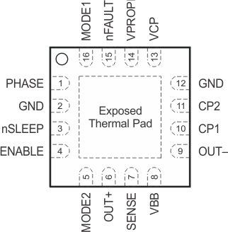
 Figure 5-1 RTY Package16-Pin QFN With Exposed Thermal PadTop View
Table 5-1 Pin Functions
| PIN | I/O | DESCRIPTION | |
|---|---|---|---|
| NAME | NO. | ||
| CP1 | 10 | PWR | Charge pump switching node. Connect a X7R, 0.1-μF, VBB-rated ceramic capacitor from CP1 to CP2. |
| CP2 | 11 | PWR | |
| ENABLE | 4 | I | Enable logic input |
| GND | 2, 12 | PWR | Ground |
| MODE 1 | 16 | I | Mode logic input |
| MODE 2 | 5 | I | Mode 2 logic input |
| nFAULT | 15 | O | Fault indication. Pulled logic low with fault condition; open-drain output requires an external pullup resistor. |
| nSLEEP | 3 | I | Sleep mode input. Logic high to enable device; logic low to enter low-power sleep mode; internal pulldown resistor. |
| OUT+ | 6 | O | DMOS full-bridge output positive |
| OUT– | 9 | O | DMOS full-bridge output negative |
| PHASE | 1 | I | Phase logic input for direction control |
| SENSE | 7 | IO | Sense power return |
| VBB | 8 | PWR | Driver supply voltage. Bypass to GND with 0.1-μF ceramic capacitors plus a bulk capacitor rated for VBB. |
| VCP | 13 | O | Charge pump reservoir capacitor pin. Connect a X7R, 0.1-μF, 16-V ceramic capacitor to VBB. |
| VPROPI | 14 | O | Winding current proportional voltage output |
| Thermal Pad | PAD | PWR | Exposed pad for thermal dissipation; connect to GND pins. |