ZHCS218F July 2011 – December 2015 DRV8804
PRODUCTION DATA.
- 1 特性
- 2 应用
- 3 说明
- 4 修订历史记录
- 5 Pin Configuration and Functions
- 6 Specifications
- 7 Detailed Description
- 8 Application and Implementation
- 9 Power Supply Recommendations
- 10Layout
- 11器件和文档支持
- 12机械、封装和可订购信息
封装选项
机械数据 (封装 | 引脚)
散热焊盘机械数据 (封装 | 引脚)
- PWP|16
订购信息
6 Specifications
6.1 Absolute Maximum Ratings
over operating free-air temperature range (unless otherwise noted)(1)| MIN | MAX | UNIT | |||
|---|---|---|---|---|---|
| VM | Power supply voltage | –0.3 | 65 | V | |
| VOUTx | Output voltage | –0.3 | 65 | V | |
| VCLAMP | Clamp voltage | –0.3 | 65 | V | |
| SDATOUT, nFAULT |
Output current | 20 | mA | ||
| Peak clamp diode current | 2 | A | |||
| DC or RMS clamp diode current | 1 | A | |||
| Digital input pin voltage | –0.5 | 7 | V | ||
| SDATOUT, nFAULT |
Digital output pin voltage | –0.5 | 7 | V | |
| Peak motor drive output current, t < 1 μs | Internally limited | A | |||
| Continuous total power dissipation | See Thermal Information | ||||
| TJ | Operating virtual junction temperature | –40 | 150 | °C | |
| Tstg | Storage temperature | –60 | 150 | °C | |
(1) All voltage values are with respect to network ground terminal.
6.2 ESD Ratings
| VALUE | UNIT | ||||
|---|---|---|---|---|---|
| V(ESD) | Electrostatic discharge | Human body model (HBM), per ANSI/ESDA/JEDEC JS-001, all pins(1) | ±3000 | V | |
| Charged device model (CDM), per JEDEC specification JESD22-C101, all pins(2) | ±1000 | ||||
(1) JEDEC document JEP155 states that 500-V HBM allows safe manufacturing with a standard ESD control process.
(2) JEDEC document JEP157 states that 250-V CDM allows safe manufacturing with a standard ESD control process.
6.3 Recommended Operating Conditions
| MIN | NOM | MAX | UNIT | ||
|---|---|---|---|---|---|
| VM | Power supply voltage | 8.2 | 60 | V | |
| VCLAMP | Output clamp voltage(2) | 0 | 60 | V | |
| IOUT | Continuous output current, single channel on, TA = 25°C, SOIC package(1) | 1.5 | A | ||
| Continuous output current, four channels on, TA = 25°C, SOIC package(1) | 0.8 | ||||
| Continuous output current, single channel on, TA = 25°C, HTSSOP package(1) | 2 | ||||
| Continuous output current, four channels on, TA = 25°C, HTSSOP package(1) | 1 | ||||
(1) Power dissipation and thermal limits must be observed.
(2) VCLAMP is used only to supply the clamp diodes. It is not a power supply input.
6.4 Thermal Information
| THERMAL METRIC(1) | DRV8804 | UNIT | ||
|---|---|---|---|---|
| DW (SOIC) | PWP (HTSSOP) | |||
| 20 PINS | 16 PINS | |||
| RθJA | Junction-to-ambient thermal resistance | 67.7 | 39.6 | °C/W |
| RθJC(top) | Junction-to-case (top) thermal resistance | 32.9 | 24.6 | °C/W |
| RθJB | Junction-to-board thermal resistance | 35.4 | 20.3 | °C/W |
| ψJT | Junction-to-top characterization parameter | 8.2 | 0.7 | °C/W |
| ψJB | Junction-to-board characterization parameter | 34.9 | 20.1 | °C/W |
| RθJC(bot) | Junction-to-case (bottom) thermal resistance | N/A | 2.3 | °C/W |
(1) For more information about traditional and new thermal metrics, see the Semiconductor and IC Package Thermal Metrics application report, SPRA953.
6.5 Electrical Characteristics
TA = 25°C, over recommended operating conditions (unless otherwise noted)| PARAMETER | TEST CONDITIONS | MIN | TYP | MAX | UNIT | |
|---|---|---|---|---|---|---|
| POWER SUPPLIES | ||||||
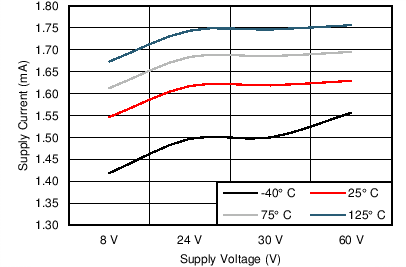
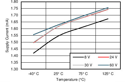
| IVM | VM operating supply current | VM = 24 V | 1.6 | 2.1 | mA | |
| VUVLO | VM undervoltage lockout voltage | VM rising | 8.2 | V | ||
| LOGIC-LEVEL INPUTS (SCHMITT TRIGGER INPUTS WITH HYSTERESIS) | ||||||
| VIL | Input low voltage | 0.6 | 0.7 | V | ||
| VIH | Input high voltage | 2 | V | |||
| VHYS | Input hysteresis | 0.45 | V | |||
| IIL | Input low current | VIN = 0 | –20 | 20 | μA | |
| IIH | Input high current | VIN = 3.3 V | 100 | μA | ||
| RPD | Pulldown resistance | 100 | kΩ | |||
| nFAULT OUTPUT (OPEN-DRAIN OUTPUT) | ||||||
| VOL | Output low voltage | IO = 5 mA | 0.5 | V | ||
| IOH | Output high leakage current | VO = 3.3 V | 1 | μA | ||
| SDATOUT OUTPUT (PUSH-PULL OUTPUT) | ||||||
| VOL | Output low voltage | IO = 5 mA | 0.5 | V | ||
| VOH | Output high voltage | IO = 100 µA, VM = 11 V - 60 V, peak | 6.5 | V | ||
| IO = 100 µA, VM = 11 V - 60 V, steady state | 3.3 | 4.5 | 5.6 | |||
| IO = 100 µA, VM = 8.2 V - 11 V, steady state | 2.5 | |||||
| ISRC | Output source current | VM = 24 V | 1 | mA | ||
| ISNK | Output sink current | VM = 24 V | 5 | mA | ||
| LOW-SIDE FETS | ||||||
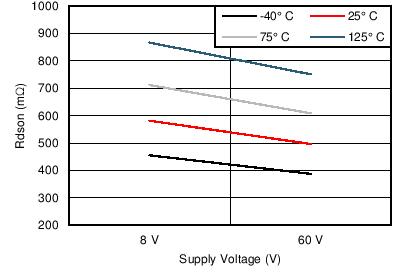
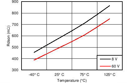
| RDS(ON) | FET on resistance | VM = 24 V, IO = 700 mA, TJ = 25°C | 0.5 | Ω | ||
| VM = 24 V, IO = 700 mA, TJ = 85°C | 0.75 | 0.8 | ||||
| IOFF | Off-state leakage current | –50 | 50 | μA | ||
| HIGH-SIDE DIODES | ||||||
| VF | Diode forward voltage | VM = 24 V, IO = 700 mA, TJ = 25°C | 1.2 | V | ||
| IOFF | Off-state leakage current | VM = 24 V, TJ = 25°C | –50 | 50 | μA | |
| OUTPUTS | ||||||
| tR | Rise time | VM = 24 V, IO = 700 mA, Resistive load | 50 | 300 | ns | |
| tF | Fall time | VM = 24 V, IO = 700 mA, Resistive load | 50 | 300 | ns | |
| PROTECTION CIRCUITS | ||||||
| IOCP | Overcurrent protection trip level | 2.3 | 3.8 | A | ||
| tOCP | Overcurrent protection deglitch time | 3.5 | µs | |||
| tRETRY | Overcurrent protection retry time | 1.2 | ms | |||
| tTSD | Thermal shutdown temperature | Die temperature(1) | 150 | 160 | 180 | °C |
(1) Not production tested.
6.6 Timing Requirements
over operating free-air temperature range (unless otherwise noted)(1)
(1) Not production tested.
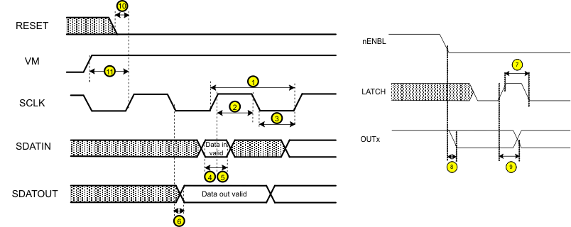
More than 400 ns of delay should exist between the final SCLK rising edge and the LATCH rising edge. This ensures that the last data bit is shifted into the device properly.
Figure 1. DRV8804 Timing Requirements
6.7 Typical Characteristics
