ZHCSBL1B September 2013 – October 2014 DRV8816
PRODUCTION DATA.
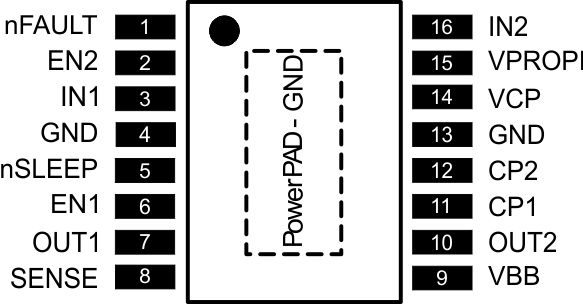
6 Pin Configuration and Functions

Pin Functions
| PIN | TYPE | DESCRIPTION | ||
|---|---|---|---|---|
| NAME | NO. | |||
| POWER AND GROUND | ||||
| CP1 | 11 | PWR | Charge pump switching node | Connect a 0.1-µF X7R capacitor rated for VBB between CP1 and CP2 |
| CP2 | 12 | — | ||
| GND | 4, 13, PPAD | PWR | Device ground | Connect to system ground |
| VBB | 9 | PWR | Power supply input | Connect to main power supply. Bypass to GND with a 0.1-µF ceramic capacitor and a larger bulk capacitor rated for at least the VBB voltage |
| VCP | 14 | PWR | Charge pump output | Connect a 0.1-µF 16-V ceramic capacitor between VCP and VBB |
| CONTROL | ||||
| EN1 | 6 | I | ½-H bridge enable | Logic high enables ½-H bridge output; logic low puts the FETs in HI-Z; internal pulldown |
| EN2 | 2 | |||
| IN1 | 3 | I | ½-H bridge control | Logic high enables the high-side ½-H bridge FET; logic low enables the low side FET; internal pulldown |
| IN2 | 16 | |||
| nFAULT | 1 | O | Fault indication pin | Pulled logic low with fault condition; open-drain output requires an external pullup |
| nSLEEP | 5 | I | Device sleep mode | Pull logic low to put device into a low-power sleep mode; internal pulldown |
| OUTPUT | ||||
| OUT1 | 7 | O | ½-H bridge output | |
| OUT2 | 10 | O | ½-H bridge output | |
| SENSE | 8 | O | H-bridge low-side connect | Connect directly to GND or through a sense resistor to set OCP |
| VPROPI | ||||
| VPROPI | 15 | O | Current-proportional output | |
Table 1. External Components
| COMPONENT | PIN 1 | PIN 2 | RECOMMENDED |
|---|---|---|---|
| CVBB | VBB | GND | 0.1-µF ceramic capacitor and a larger bulk capacitor rated for at least the VBB voltage |
| CVCP | VCP | VBB | 0.1-µF 16-V ceramic capacitor |
| RnFAULT | VCC(1) | nFAULT | >1 kΩ resistor |
| RnSLEEP | VCC(1) | nSLEEP | If nSLEEP isn't actively controlled, use a pull-up resistor of less than 20 kΩ |
| RSENSE | SENSE | GND | Optional low-value resistor. If not used, connect SENSE pin directly to GND. |
| RVPROPI | VPROPI | GND | If VPROPI is used, add a 100kΩ resistor to GND |
(1) VCC is not a pin on the DRV8816, but a VCC supply voltage pullup is required.