ZHCSBL1B September 2013 – October 2014 DRV8816
PRODUCTION DATA.
7 Specifications
7.1 Absolute Maximum Ratings(1)
over operating free-air temperature range (unless otherwise noted)| MIN | MAX | UNIT | ||
|---|---|---|---|---|
| VBB | Power supply voltage | –0.6 | 40 | V |
| Charge pump positive switching pin (CP2) | –0.6 | VBB + 7 | V | |
| Charge pump negative switching pin (CP1) | –0.6 | VBB | V | |
| Digital pin voltage range (IN1, IN2, EN1, EN2, nSLEEP, nFAULT) | –0.3 | 7 | V | |
| VBB to OUTx | –0.6 | 40 | V | |
| OUTx to SENSE | –0.6 | 40 | V | |
| V(SENSE) | Sense voltage (SENSE) (2) | –0.5 | 1.0 | V |
| H-bridge output current (OUT1, OUT2, SENSE) | 0 | 2.8 | A | |
| VPROPI pin voltage range (VPROPI) | –0.3 | 3.6 | V | |
| TA | Operating ambient temperature | –40 | 85 | °C |
| TJ | Operating junction temperature | –40 | 190 | |
(1) Stresses beyond those listed under “absolute maximum ratings” may cause permanent damage to the device. These are stress ratings only, and functional operation of the device at these or any other conditions beyond those indicated under “recommended operating conditions” is not implied. Exposure to absolute-maximum-rated conditions for extended periods may affect device reliability.
(2) Transients of ±1 V for less than 25 ns are acceptable.
7.2 Handling Ratings
| MIN | MAX | UNIT | |||
|---|---|---|---|---|---|
| Tstg | Storage temperature range | –40 | 125 | °C | |
| V(ESD) | Electrostatic discharge | Human body model (HBM), per ANSI/ESDA/JEDEC JS-001, all pins(1) | –2000 | 2000 | V |
| Charged device model (CDM), per JEDEC specification JESD22-C101, all pins(2) | –500 | 500 | |||
(1) JEDEC document JEP155 states that 500-V HBM allows safe manufacturing with a standard ESD control process.
(2) JEDEC document JEP157 states that 250-V CDM allows safe manufacturing with a standard ESD control process.
7.3 Recommended Operating Conditions(1)
| MIN | MAX | UNIT | ||
|---|---|---|---|---|
| VBB | Power supply voltage range | 8 | 38 | V |
| VI | Input pin voltage range | 0 | 5.5 | V |
| fPWM | Applied PWM signal (IN1, IN2, EN1, EN2) | 100 | kHz | |
| IOUT | H-bridge output current | 2.8 | A | |
| TA | Ambient temperature | –40 | 85 | °C |
(1) Power dissipation and thermal limits must be observed.
7.4 Thermal Information
| THERMAL METRIC(1) | DRV8816 | UNIT | |
|---|---|---|---|
| PWP | |||
| 16 PINS | |||
| RθJA | Junction-to-ambient thermal resistance(2) | 43.9 | °C/W |
| RθJC(top) | Junction-to-case (top) thermal resistance(3) | 30.8 | |
| RθJB | Junction-to-board thermal resistance(4) | 25.3 | |
| ψJT | Junction-to-top characterization parameter(5) | 1.1 | |
| ψJB | Junction-to-board characterization parameter(6) | 25 | |
| RθJC(bot) | Junction-to-case (bottom) thermal resistance(7) | 5.6 | |
(1) For more information about traditional and new thermal metrics, see the IC Package Thermal Metrics application report, SPRA953.
(2) The junction-to-ambient thermal resistance under natural convection is obtained in a simulation on a JEDEC-standard, high-K board, as specified in JESD51-7, in an environment described in JESD51-2a.
(3) The junction-to-case (top) thermal resistance is obtained by simulating a cold plate test on the package top. No specific JEDEC- standard test exists, but a close description can be found in the ANSI SEMI standard G30-88.
(4) The junction-to-board thermal resistance is obtained by simulating in an environment with a ring cold plate fixture to control the PCB temperature, as described in JESD51-8.
(5) The junction-to-top characterization parameter, ψ JT , estimates the junction temperature of a device in a real system and is extracted from the simulation data for obtaining θ JA , using a procedure described in JESD51-2a (sections 6 and 7).
(6) The junction-to-board characterization parameter, ψ JB , estimates the junction temperature of a device in a real system and is extracted from the simulation data for obtaining θ JA , using a procedure described in JESD51-2a (sections 6 and 7).
(7) The junction-to-case (bottom) thermal resistance is obtained by simulating a cold plate test on the exposed (power) pad. No specific JEDEC standard test exists, but a close description can be found in the ANSI SEMI standard G30-88.
7.5 Electrical Characteristics
over recommended operating conditions (unless otherwise noted)| PARAMETER | TEST CONDITIONS | MIN | TYP | MAX | UNIT | ||
|---|---|---|---|---|---|---|---|
| POWER SUPPLIES (VBB) | |||||||
| VBB | VBB operating voltage | 8 | 38 | V | |||
| IVBB | VBB operating supply current | ƒPWM < 50 kHz | 6 | mA | |||
| Charge pump on, Outputs disabled | 3.2 | mA | |||||
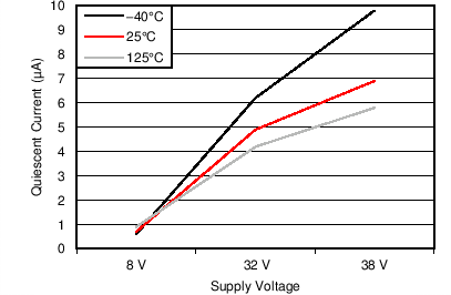
| IVBBQ | VBB sleep-mode supply current | nSLEEP = 0, TJ = 25°C | 10 | µA | |||
| CONTROL INPUTS (IN1, IN2, EN1, EN2, nSLEEP) | |||||||
| VIL | Input logic low voltage | IN1, IN2, EN1, EN2 | 0 | 0.8 | V | ||
| VIH | Input logic high voltage | 2 | 5.5 | ||||
| VIL | Input logic low voltage | nSLEEP | 0 | 0.8 | V | ||
| VIH | Input logic high voltage | 2.2 | 5.5 | V | |||
| IIL | Input logic low current | IN1, IN2, EN2, nSLEEP | VIN = 0 V | 0 | μA | ||
| IIH | Input logic high current | VIN = 5 V | 25 | ||||
| IIL | Input logic low current | EN1 | VIN = 0 V | 0 | μA | ||
| IIH | Input logic high current | VIN = 5 V | 100 | ||||
| RPD | Pulldown resistance | IN1, IN2, EN2, nSLEEP | 200 | kΩ | |||
| EN1 | 50 | ||||||
| SERIAL AND CONTROL OUTPUT (nFAULT) | |||||||
| VOL | Output logic low voltage | Isink = 1 mA | 0.4 | V | |||
| DMOS DRIVERS (OUT1, OUT2, SENSE) | |||||||
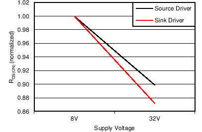
| RDS(on) | Output ON resistance | Source driver, IOUT = –2.8 A, TJ = 25°C | 0.48 | Ω | |||
| Source driver, IOUT = –2.8 A, TJ = 125°C | 0.74 | 0.85 | |||||
| Sink driver, IOUT = –2.8 A, TJ = 25°C | 0.35 | ||||||
| Sink driver, IOUT = –2.8 A, TJ = 125°C | 0.52 | 0.7 | |||||
| VTRIP | SENSE trip voltage | RSENSE between SENSE and GND | 500 | mV | |||
| Vf | Body diode forward voltage | Source diode, If = –2.8 A | 1.4 | V | |||
| Sink diode, If = 2.8 A | 1.4 | ||||||
| tpd | OUTx propagation delay | From High-Z to High | 70 | ns | |||
| From High-Z to Low | 700(2) | ||||||
| From High to High-Z | 120 | ||||||
| From High to Low | 700 | ||||||
| From Low to High-Z | 350 | ||||||
| From Low to High | 350 | ||||||
| tCOD | Crossover delay | 500 | ns | ||||
| DAGain | VPROPI amplifier gain | Sense = 0.1 to 0.4 V | 5 | V/V | |||
| PROTECTION CIRCUITS | |||||||
| VUVLO | VBB UVLO | VBB rising | 6.5 | 7.5 | V | ||
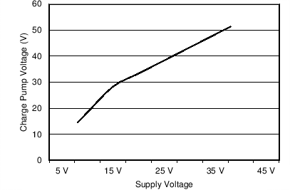
| VCPUV | VCP UVLO(1) | VBB rising; CPUV recovery | 12 | 13.8 | V | ||
| IOCP | Overcurrent protection trip level | 3 | A | ||||
| tDEG | Overcurrent deglitch time | 3.0 | µs | ||||
| tOCP | Overcurrent retry time | 1.6 | ms | ||||
| TOTW | Thermal warning temperature | Die temperature Tj | 160 | °C | |||
| TOTW HYS | Thermal warning hysteresis | Die temperature Tj | 15 | °C | |||
| TOTS | Thermal shutdown temperature | Die temperature Tj | 175 | °C | |||
| TOTS HYS | Thermal shutdown hysteresis | Die temperature Tj | 15 | °C | |||
(1) Whenever VCP is less than VM + 10 V, a CPUV event occurs. This fault will be asserted whenever VBB is below 12 V. Note that the H-bridges will remain enabled until VBB = VUVLO even through nFAULT is pulled low.
(2) If OUT2 is High, the typical time for OUT1 to go from High-Z to Low is 1700 ns.
7.6 Typical Characteristics


