SLVSBW9C April 2013 – December 2015 DRV8832-Q1
PRODUCTION DATA.
- 1 Features
- 2 Applications
- 3 Description
- 4 Revision History
- 5 Pin Configuration and Functions
- 6 Specifications
- 7 Detailed Description
- 8 Application and Implementation
- 9 Power Supply Recommendations
- 10Layout
- 11Device and Documentation Support
- 12Mechanical, Packaging, and Orderable Information
封装选项
请参考 PDF 数据表获取器件具体的封装图。
机械数据 (封装 | 引脚)
- DGQ|10
散热焊盘机械数据 (封装 | 引脚)
- DGQ|10
订购信息
8.2.3 Application Curves
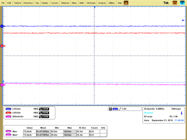
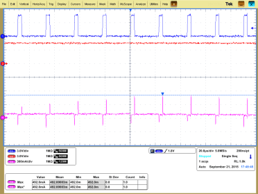
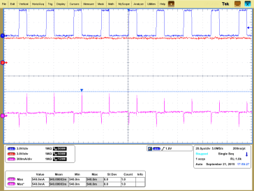
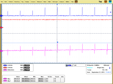
The following scope captures show how the output duty cycle changes to as VCC increases. This allows the motor to spin at a constant speed as VCC changes. At VCC = 3.9 V, the output duty cycle is 100% on. As the VCC voltage increases to greater than 4 V, the output duty cycle begins to decrease. The output duty cycle is shown at VCC = 4.5 V, VCC = 5 V and VCC = 5.5 V.
- Channel 1 – OUT1: IN1 – Logic Low
- Channel 2 – OUT2: IN2 – Logic High
- Channel 4 – Motor current: VSET – 1 V
- Motor used: NMB Technologies Corporation, PPN7PA12C1
 Figure 10. Output Pulse Width Modulating at VCC = 3.9 V
  Figure 12. Output Pulse Width Modulating at VCC = 4.5 V
  Figure 14. Output Pulse Width Modulating at VCC = 5.5 V
  Figure 11. Output Pulse Width Modulating at VCC = 4 V
  Figure 13. Output Pulse Width Modulating at VCC = 5 V