SLVSB19D February 2012 – March 2015 DRV8834
PRODUCTION DATA.
- 1 Features
- 2 Applications
- 3 Description
- 4 Simplified Schematic
- 5 Revision History
- 6 Pin Configuration and Functions
- 7 Specifications
- 8 Detailed Description
- 9 Application and Implementation
- 10Power Supply Recommendations
- 11Layout
- 12Device and Documentation Support
- 13Mechanical, Packaging, and Orderable Information
封装选项
机械数据 (封装 | 引脚)
散热焊盘机械数据 (封装 | 引脚)
订购信息
9 Application and Implementation
NOTE
Information in the following applications sections is not part of the TI component specification, and TI does not warrant its accuracy or completeness. TI’s customers are responsible for determining suitability of components for their purposes. Customers should validate and test their design implementation to confirm system functionality.
9.1 Application Information
The DRV8834 is a very flexible motor driver. It can be used to drive two DC motors or a stepper motor, in a number of different configurations.
The following applications schematics show various configurations and connections for the DRV8834.
Component values, especially for RSENSE and the DECAY pins, may be different depending on your motor and application. Refer to the information above to determine the best values for these components in your application.
9.1.1 Sense Resistor
For optimal performance, it is important for the sense resistor to be:
- Surface-mount
- Low inductance
- Rated for high enough power
- Placed closely to the motor driver
The power dissipated by the sense resistor equals IRMS2 × R. For example, if peak motor current is 3 A, RMS motor current is 2 A, and a 0.05-Ω sense resistor is used, the resistor will dissipate 2A2 × 0.05 Ω = 0.2 W. The power quickly increases with higher current levels.
Resistors typically have a rated power within some ambient temperature range, along with a derated power curve for high ambient temperatures. When a PCB is shared with other components generating heat, margin should be added. It is always best to measure the actual sense resistor temperature in a final system, along with the power MOSFETs, as those are often the hottest components.
Because power resistors are larger and more expensive than standard resistors, it is common practice to use multiple standard resistors in parallel, between the sense node and ground. This distributes the current and heat dissipation.
9.2 Typical Application
9.2.1 Phase/Enable Mode Driving Two DC Motors
In this configuration, the DRV8834 is used to drive two independent DC motors. Current up to 1 A per motor is possible. The M1 pin is pulled low to allow slow decay PWM from the controller (if desired) to control the motor speed by PWMing the xENBL inputs, and ADECAY and BDECAY are connected to ground to set slow decay mode during current limiting. The value of the RSENSE resistors shown is for a 1-A current limit; if current limiting is not needed, the AISEN and BISEN pins may be connected directly to ground. If the sleep function is not needed, nSLEEP can be connected to VM with an approximate 47-kΩ resistor.
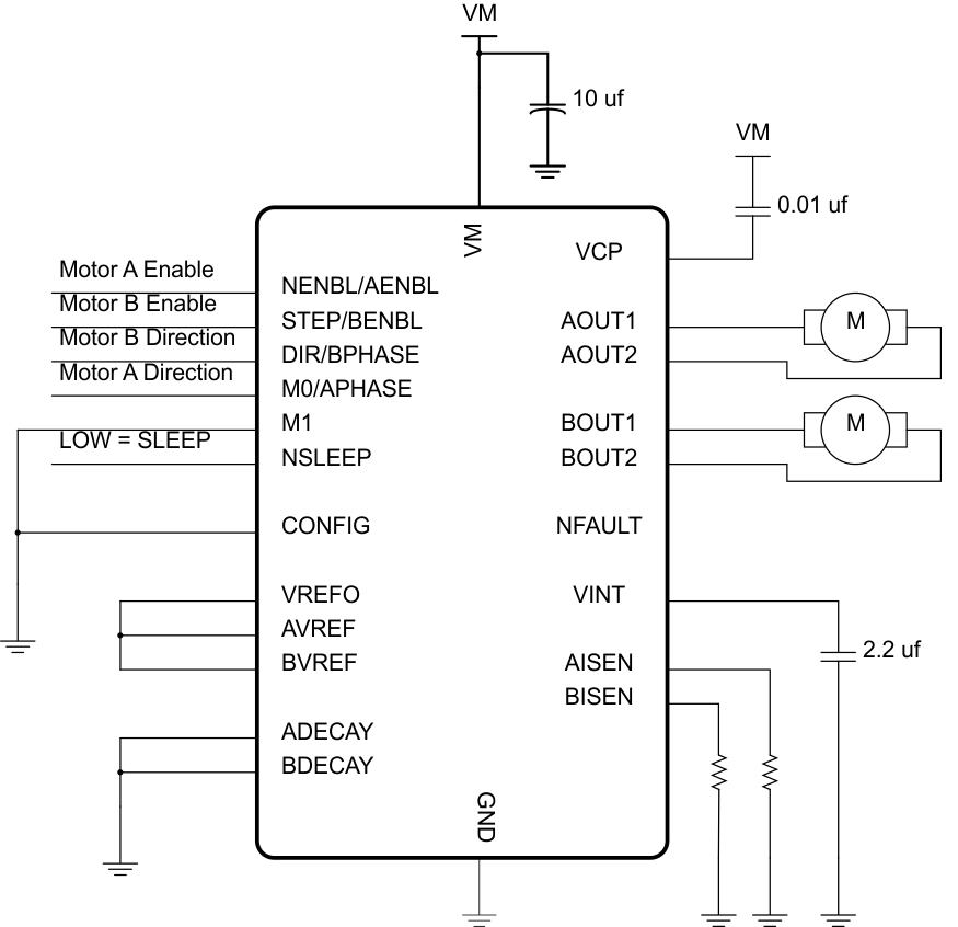 Figure 9. Phase/Enable Mode Driving Two DC Motors
9.2.1.1 Design Requirements
Table 5 lists the design parameters.
Table 5. Design Parameters
| PARAMETER | REFERENCE | EXAMPLE VALUE |
|---|---|---|
| Motor voltage | VM | 10 V |
| Motor RMS current | IRMS | 0.8 A |
| Motor start-up current | ISTART | 1 A |
| Motor current trip point | ITRIP | 1.5 A |
9.2.1.2 Detailed Design Procedure
9.2.1.2.1 Motor Voltage
The motor voltage to use will depend on the ratings of the motor selected and the desired RPM. A higher voltage spins a brushed DC motor faster with the same PWM duty cycle applied to the power FETs. A higher voltage also increases the rate of current change through the inductive motor windings.
9.2.1.2.2 Power Dissipation
The power dissipation of the DRV8834 is a function of RMS motor current and the FET resistance (RDS(ON)) of each output.
For this example, the ambient temperature is 35°C, and the junction temperature reaches 65°C. At 65°C, the sum of RDS(ON) is about 1 Ω. With an example motor current of 0.8 A, the dissipated power in the form of heat will be 0.8 A2 × 1 Ω = 0.64 W.
The temperature that the DRV8834 reaches will depend on the thermal resistance to the air and PCB. It is important to solder the device PowerPAD to the PCB ground plane, with vias to the top and bottom board layers, in order dissipate heat into the PCB and reduce the device temperature. In the example used here, the DRV8834 had an effective thermal resistance RθJA of 47°C/W, and:
9.2.1.2.3 Motor Current Trip Point
When the voltage on pin SENSE exceeds VTRIP (0.5 V), overcurrent is detected. The RSENSE resistor should be sized to set the desired ITRIP level.
To set ITRIP to 2 A, RSENSE = 0.5 V / 2 A = 0.25 Ω.
To prevent false trips, ITRIP must be higher than regular operating current. Motor current during start-up is typically much higher than steady-state spinning, because the initial load torque is higher, and the absence of back-EMF causes a higher voltage and extra current across the motor windings.
It can be beneficial to limit start-up current by using series inductors on the DRV8834 output, as that allows ITRIP to be lower, and it may decrease the system’s required bulk capacitance. Start-up current can also be limited by ramping the forward drive duty cycle.
9.2.1.3 Application Curves
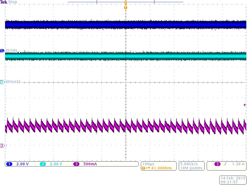 Figure 10. Brushed Motor – VM = 8 V,
DRV8834 is Regulating Current
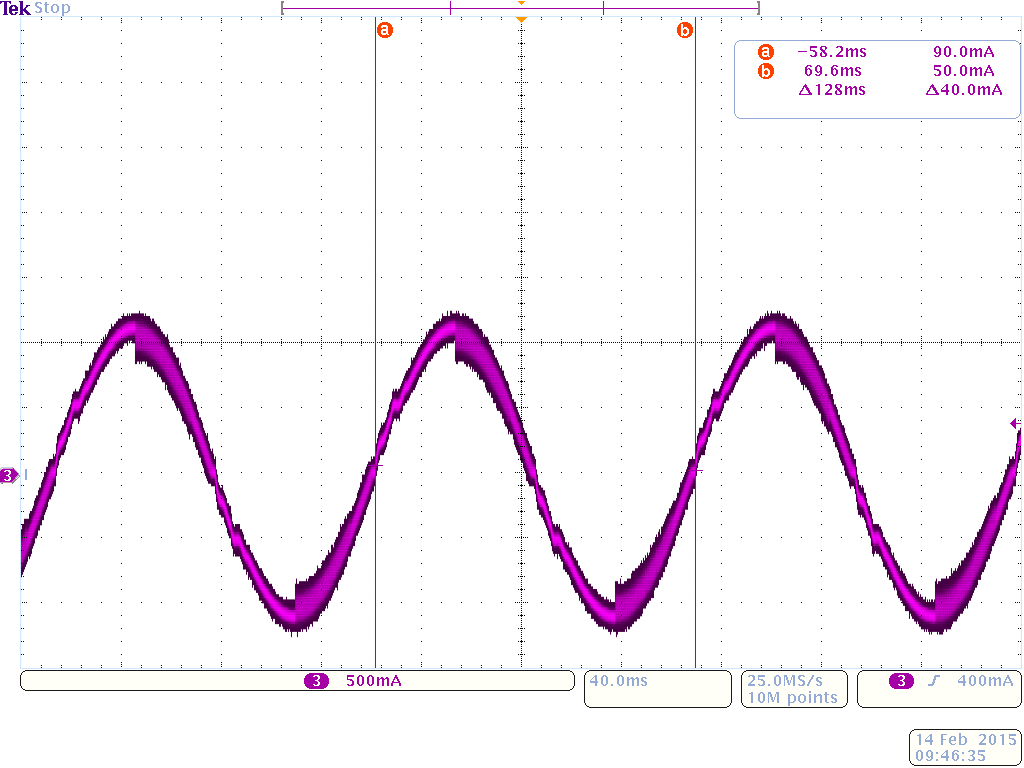 Figure 12. External Microstepping – VM = 8 V, 4000 Steps Per Second,
 1/128 microstep mode, 1.2-A Current Regulation
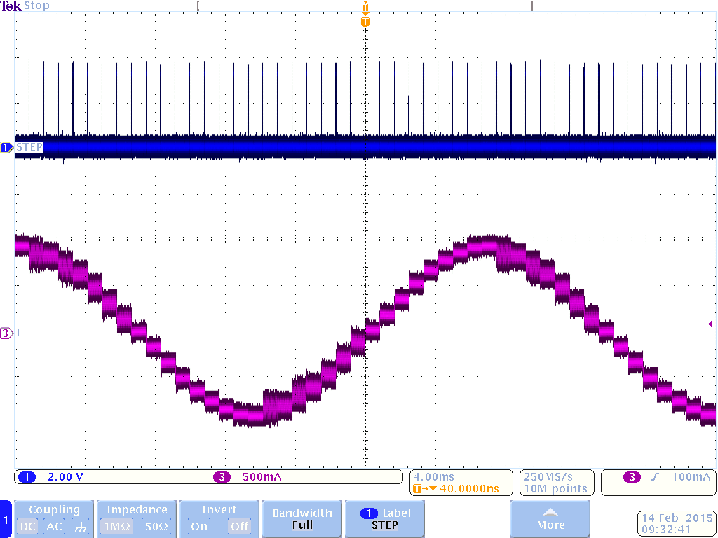 Figure 11. Internal Indexer – VM = 8 V, 1200 Steps per
 second, 1/8 microstep mode, 1-A Current regulation
9.2.2 Phase/Enable Mode Driving a Stepper Motor
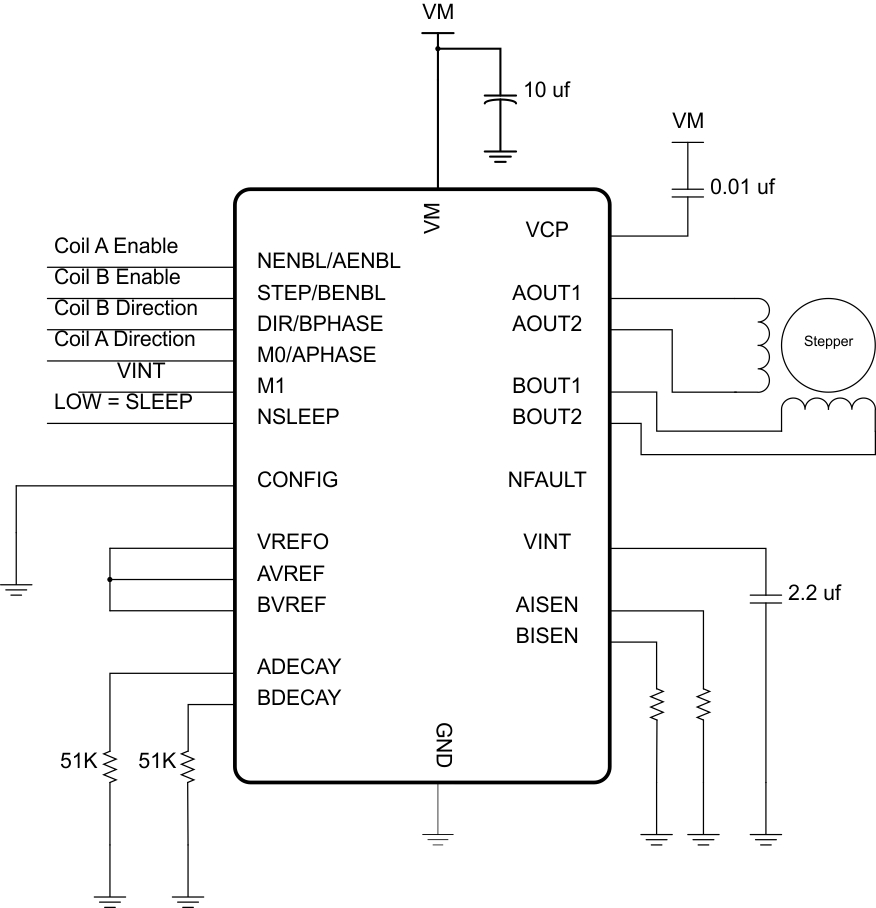 Figure 13. Phase/Enable Mode Driving a Stepper Motor
9.2.2.1 Design Requirements
Table 6 lists the design parameters.
Table 6. Design Parameters
| PARAMETER | REFERENCE | EXAMPLE VALUE |
|---|---|---|
| Supply voltage | VM | 6 V |
| Motor winding resistance | RL | 3.9 Ω |
| Motor winding inductance | IL | 2.9 mH |
| Motor full step angle | θstep | 1.8°/step |
| Target microstepping level | nm | 2 µsteps per step |
| Target motor speed | V | 120 RPM |
| Target full-scale current | IFS | 1.25 A |
9.2.2.2 Detailed Design Procedure
Phase/enable mode can be used with a simple interface to a controller to operate a stepper motor in full or half step modes. The decay mode can be set by changing the values of the resistors connected to the ADECAY and BDECAY pins. The M1 pin is driven to logic high (by connecting to the VINT supply), to allow a zero-current (off) state when the xENBL pin is set low. Coil current is set by the RSENSE resistors. If the sleep function is not needed, nSLEEP can be connected to VM with an approximate 47-kΩ resistor.
9.2.2.2.1 Stepper Motor Speed
The first step in configuring the DRV8834 requires the desired motor speed and microstepping level. If the target application requires a constant speed, then a square wave with frequency ƒstep must be applied to the STEP pin.
If the target motor start-up speed is too high, the motor will not spin. Make sure that the motor can support the target speed or implement an acceleration profile to bring the motor up to speed.
For a desired motor speed (v), microstepping level (nm), and motor full step angle (θstep),
θstep can be found in the stepper motor data sheet or written on the motor itself.
For the DRV8834, the microstepping level is set by the MODE pins and can be any of the settings in Table 6. Higher microstepping will mean a smoother motor motion and less audible noise, but will increase switching losses and require a higher fstep to achieve the same motor speed.
9.2.2.2.2 Current Regulation
In a stepper motor, the set full-scale current (IFS) is the maximum current driven through either winding. This quantity will depend on the xVREF analog voltage and the sense resistor value (RSENSE). During stepping, IFS defines the current chopping threshold (ITRIP) for the maximum current step. The gain of DRV8834 is set for 5 V/V.
To achieve IFS = 1.25 A with RSENSE of 0.2 Ω, xVREF should be 1.25 V.
9.2.2.2.3 Decay Modes
The DRV8834 supports three different decay modes: slow decay, fast decay, and mixed decay. The current through the motor windings is regulated using a fixed-frequency PWM scheme. This means that after any drive phase, when a motor winding current has hit the current chopping threshold (ITRIP), the DRV8834 will place the winding in one of the three decay modes until the PWM cycle has expired. Afterward, a new drive phase starts.
The blanking time TBLANK defines the minimum drive time for the current chopping. ITRIP is ignored during TBLANK, so the winding current may overshoot the trip level.
9.2.2.3 Application Curves
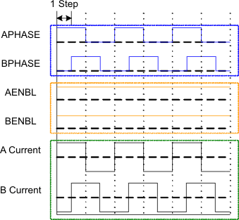 Figure 14. Full Step Sequence (2-Phase)
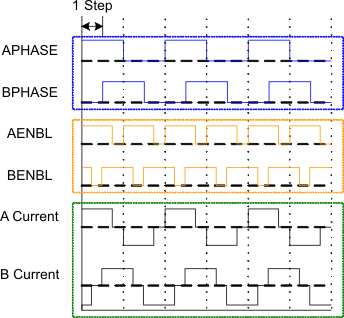 Figure 15. Half Step Sequence (1-2 Phase)
9.2.3 Indexer Mode Driving a Stepper Motor
In indexer mode, only a rising edge on the STEP pin is needed to move the motor to the next step. The DIR pin sets which direction the motor rotates, by reversing the step sequence. The internal indexer can operate in full-step, half-step, and smaller microsteps up to 1/32-step, depending on the state of the M0 and M1 pins. The M0 and M1 pins can also be connected directly to ground or to VINT to program the step modes, if desired. If the sleep function is not needed, nSLEEP can be connected to VM with an approximate 47-kΩ resistor. Step sequences for full and half step are shown below.
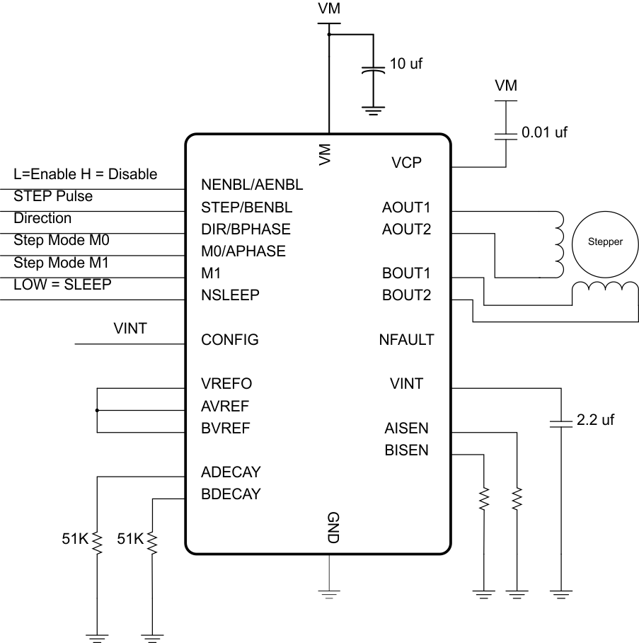 Figure 16. Indexer Mode Driving a Stepper Motor
9.2.3.1 Design Requirements
Table 7 lists the design parameters.
Table 7. Design Parameters
| PARAMETER | REFERENCE | EXAMPLE VALUE |
|---|---|---|
| Supply Voltage | VM | 6 V |
| Motor Winding Resistance | RL | 3.9 Ω |
| Motor Winding Inductance | IL | 2.9 mH |
| Motor Full Step Angle | θstep | 1.8°/step |
| Target Microstepping Level | nm | 8 µsteps per step |
| Target Motor Speed | V | 120 RPM |
| Target Full-Scale Current | IFS | 1.25 A |
9.2.3.2 Detailed Design Procedures
Phase/enable mode can be used with a simple interface to a controller to operate a stepper motor in full or half step modes. The decay mode can be set by changing the values of the resistors connected to the ADECAY and BDECAY pins. The M1 pin is driven to logic high (by connecting to the VINT supply), to allow a zero-current (off) state when the xENBL pin is set low. Coil current is set by the RSENSE resistors. If the sleep function is not needed, nSLEEP can be connected to VM with an approximate 47-kΩ resistor.
9.2.3.2.1 Stepper Motor Speed
The first step in configuring the DRV8834 requires the desired motor speed and microstepping level. If the target application requires a constant speed, then a square wave with frequency ƒstep must be applied to the STEP pin.
If the target motor start-up speed is too high, the motor will not spin. Make sure that the motor can support the target speed or implement an acceleration profile to bring the motor up to speed.
For a desired motor speed (v), microstepping level (nm), and motor full step angle (θstep),
θstep can be found in the stepper motor data sheet or written on the motor itself.
For the DRV8834, the microstepping level is set by the MODE pins and can be any of the settings in Table 6. Higher microstepping will mean a smoother motor motion and less audible noise, but will increase switching losses and require a higher fstep to achieve the same motor speed.
9.2.3.2.2 Current Regulation
In a stepper motor, the set full-scale current (IFS) is the maximum current driven through either winding. This quantity will depend on the xVREF analog voltage and the sense resistor value (RSENSE). During stepping, IFS defines the current chopping threshold (ITRIP) for the maximum current step. The gain of DRV8834 is set for 5 V/V.
To achieve IFS = 1.25 A with RSENSE of 0.2 Ω, xVREF should be 1.25 V.
9.2.3.2.3 Decay Modes
The DRV8834 supports three different decay modes: slow decay, fast decay, and mixed decay. The current through the motor windings is regulated using a fixed-frequency PWM scheme. This means that after any drive phase, when a motor winding current has hit the current chopping threshold (ITRIP), the DRV8834 will place the winding in one of the three decay modes until the PWM cycle has expired. Afterward, a new drive phase starts.
The blanking time TBLANK defines the minimum drive time for the current chopping. ITRIP is ignored during TBLANK, so the winding current may overshoot the trip level.
9.2.3.3 Application Curves
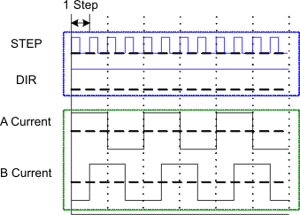 Figure 17. Full Step Sequence (2-Phase)
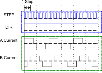 Figure 18. Half Step Sequence (1-2 Phase)
9.2.4 High-Resolution Microstepping Using a Microcontroller to Modulate VREF Signals
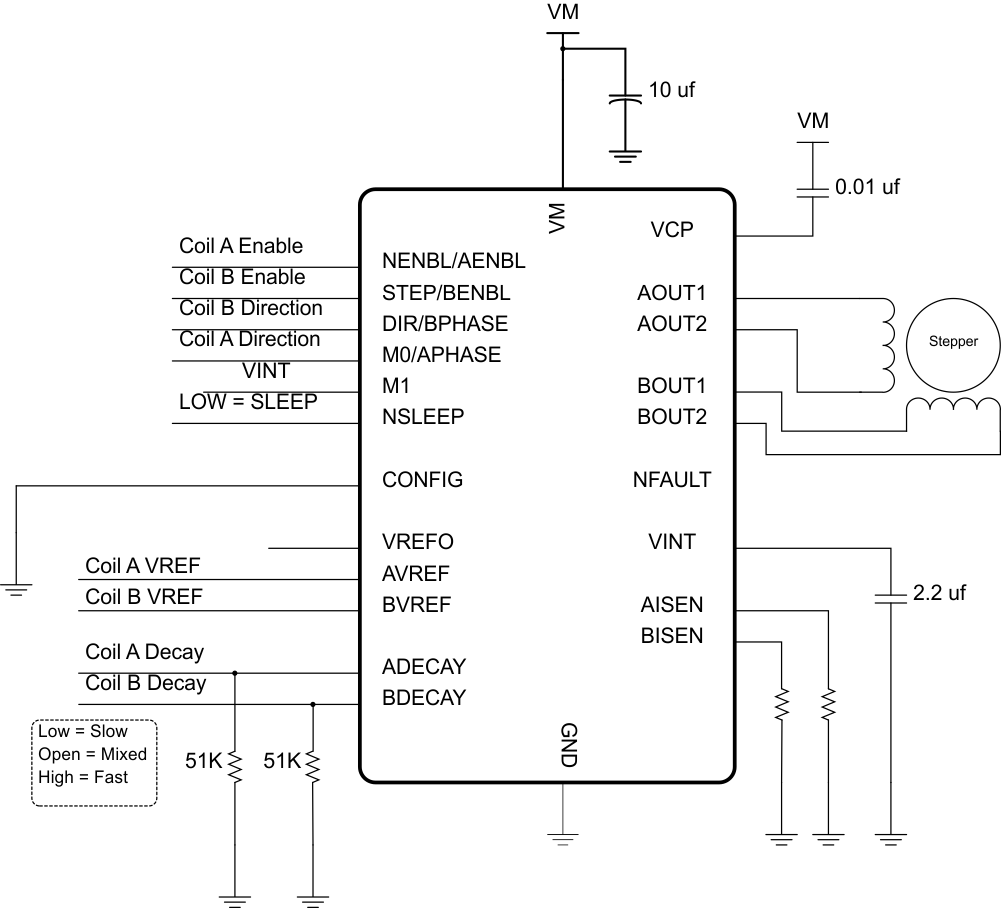 Figure 19. High-Resolution Microstepping
9.2.4.1 Design Requirements
Table 8 lists the design parameters.
Table 8. Design Parameters
| PARAMETER | REFERENCE | EXAMPLE VALUE |
|---|---|---|
| Supply voltage | VM | 6 V |
| Motor winding resistance | RL | 3.9 Ω |
| Motor winding inductance | IL | 2.9 mH |
| Motor full step angle | θstep | 1.8°/step |
| Target microstepping level | nm | 128 µsteps per step |
| Target motor speed | V | 120 RPM |
| Target full-scale current | IFS | 1.25 A |
9.2.4.2 Detailed Design Procedure
Using a microcontroller with two DAC outputs, very high resolution microstepping can be performed with the DRV8834. In this mode, the coil current direction is controlled by the PHASE pins, and the current in each coil is independently set using the two VREF input pins, which are connected to DACs. In addition, the microcontroller can set the decay mode for each coil dynamically, by driving the xDECAY pin low for slow decay, high for fast decay, or high-impedance which sets mixed decay (based on the value of a resistor connected to ground). If the sleep function is not needed, nSLEEP can be connected to VM with an approximate 47-kΩ resistor.
For more details on this technique, refer to TI Application Report, High Resolution Microstepping Driver With the DRV88xx Series (SLVA416).
9.2.4.3 Application Curves
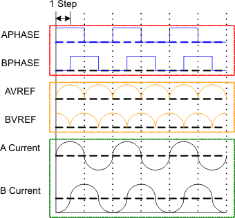 Figure 20. Microstepping Sequence
 Figure 22. Half Step Sequence (1-2 Phase)
 Figure 21. Full Step Sequence (2-Phase)