SLVSB18H March 2012 – August 2016 DRV8835
PRODUCTION DATA.
7 Detailed Description
7.1 Overview
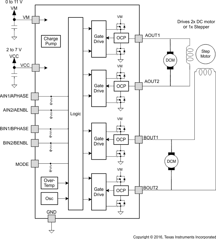
The DRV8835 is an integrated motor-driver solution used for brushed motor control. The device integrates two
H-bridges, and drives two DC motor or one stepper motor. The output driver block for each H-bridge consists of
N-channel power MOSFETs. An internal charge pump generates the gate drive voltages. Protection features include overcurrent protection, short circuit protection, undervoltage lockout, and overtemperature protection.
The bridges connect in parallel for additional current capability.
The DRV8835 allows separation of the motor voltage and logic voltage if desired. If VM and VCC are less than
7 V, the two voltages can be connected.
The mode pin allow selection of either a PHASE/ENABLE or IN/IN interface.
7.2 Functional Block Diagram

7.3 Feature Description
7.3.1 Protection Circuits
The DRV8835 is fully protected against undervoltage, overcurrent, and overtemperature events.
7.3.1.1 Overcurrent Protection (OCP)
An analog current limit circuit on each FET limits the current through the FET by removing the gate drive. If this analog current limit persists for longer than the OCP time, all FETs in the H-bridge disable. After approximately
1 ms, the bridge re-enable automatically.
Overcurrent conditions on both high-side and low-side devices; a short to ground, supply, or across the motor winding result in an overcurrent shutdown.
7.3.1.2 Thermal Shutdown (TSD)
If the die temperature exceeds safe limits, all FETs in the H-bridge disable. Operation automatically resumes once the die temperature falls to a safe level.
7.3.1.3 Undervoltage Lockout (UVLO)
If at any time the voltage on the VCC pins falls below the undervoltage lockout threshold voltage, all circuitry in the device disable, and internal logic resets. Operation resumes when VCC rises above the UVLO threshold.
Table 1. Device Protection
| FAULT | CONDITION | ERROR REPORT | H-BRIDGE | INTERNAL CIRCUITS | RECOVERY |
|---|---|---|---|---|---|
| VCC undervoltage (UVLO) | VCC < VUVLO | None | Disabled | Disabled | VCC > VUVLO |
| Overcurrent (OCP) | IOUT > IOCP | None | Disabled | Operating | tOCR |
| Thermal Shutdown (TSD) | TJ > TTSD | None | Disabled | Operating | TJ < TTSD – THYS |
7.4 Device Functional Modes
The DRV8835 is active when the VCC is set to a logic high. When in sleep mode, the H-bridge FETs are disabled (HIGH-Z).
Table 2. Device Operating Modes
| OPERATING MODE | CONDITION | H-BRIDGE | INTERNAL CIRCUITS |
|---|---|---|---|
| Operating | nSLEEP high | Operating | Operating |
| Sleep mode | nSLEEP low | Disabled | Disabled |
| Fault encountered | Any fault condition met | Disabled | See Table 1 |
7.4.1 Bridge Control
Two control modes are available in the DRV8835: IN/IN mode, and PHASE/ENABLE mode. IN/IN mode is selected if the MODE pin is driven low or left unconnected; PHASE/ENABLE mode is selected if the MODE pin is driven to logic high. Table 3 and Table 4 show the logic for these modes.
Table 3. IN/IN Mode
| MODE | xIN1 | xIN2 | xOUT1 | xOUT2 | FUNCTION (DC MOTOR) |
|---|---|---|---|---|---|
| 0 | 0 | 0 | Z | Z | Coast |
| 0 | 0 | 1 | L | H | Reverse |
| 0 | 1 | 0 | H | L | Forward |
| 0 | 1 | 1 | L | L | Brake |
Table 4. Phase/Enable Mode
| MODE | xENABLE | xPHASE | xOUT1 | xOUT2 | FUNCTION (DC MOTOR) |
|---|---|---|---|---|---|
| 1 | 0 | X | L | L | Brake |
| 1 | 1 | 1 | L | H | Reverse |
| 1 | 1 | 0 | H | L | Forward |
7.4.2 Sleep Mode
If the VCC pin reaches 0 V, the DRV8835 enters a low-power sleep mode. In this state all unnecessary internal circuitry powers down. For minimum supply current, all inputs should be low (0 V) during sleep mode.