SLVSB17D March 2012 – April 2016 DRV8836
PRODUCTION DATA.
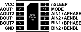
5 Pin Configuration and Functions
DSS Package
12-Pin WSON
Top View

Pin Functions
| PIN | I/O(1) | DESCRIPTION | EXTERNAL COMPONENTS OR CONNECTIONS |
|
|---|---|---|---|---|
| NAME | NO. | |||
| POWER AND GROUND | ||||
| GND, Thermal pad | 6 | — | Device ground | |
| VCC | 1 | — | Device and motor supply | Bypass to GND with a 0.1-μF (minimum) ceramic capacitor |
| CONTROL | ||||
| AIN1/APHASE | 10 | I | Bridge A input 1/PHASE input | IN/IN mode: Logic high sets AOUT1 high PH/EN mode: Sets direction of H-bridge A Internal pulldown resistor |
| AIN2/AENBL | 9 | I | Bridge A input 2/ENABLE input | IN/IN mode: Logic high sets AOUT2 high PH/EN mode: Logic high enables H-bridge A Internal pulldown resistor |
| BIN1/BPHASE | 8 | I | Bridge B input 1/PHASE input | IN/IN mode: Logic high sets BOUT1 high PH/EN mode: Sets direction of H-bridge B Internal pulldown resistor |
| BIN2/BENBL | 7 | I | Bridge B input 2/ENABLE input | IN/IN mode: Logic high sets BOUT2 high PH/EN mode: Logic high enables H-bridge B Internal pulldown resistor |
| MODE | 11 | I | Input mode select | Logic low selects IN/IN mode Logic high selects PH/EN mode Internal pulldown resistor |
| nSLEEP | 12 | I | Sleep input | Active low places part in low-power sleep state Internal pulldown resistor |
| OUTPUT | ||||
| AOUT1 | 2 | O | Bridge A output 1 | Connect to motor winding A |
| AOUT2 | 3 | O | Bridge A output 2 | |
| BOUT1 | 4 | O | Bridge B output 1 | Connect to motor winding B |
| BOUT2 | 5 | O | Bridge B output 2 | |
(1) Directions: I = input, O = output, OZ = tri-state output, OD = open-drain output, IO = input/output.