ZHCSCM3 July   2014 DRV8842-EP

PRODUCTION DATA.  

  1. 特性
  2. 应用范围
  3. 说明
  4. 简化电路原理图
  5. 修订历史记录
  6. Pin Configuration and Functions
  7. Specifications
    1. 7.1 Absolute Maximum Ratings
    2. 7.2 Handling Ratings
    3. 7.3 Recommended Operating Conditions
    4. 7.4 Thermal Information
    5. 7.5 Electrical Characteristics
    6. 7.6 Motor Driver Timing Requirements
    7. 7.7 Typical Characteristics
  8. Detailed Description
    1. 8.1 Overview
    2. 8.2 Functional Block Diagram
    3. 8.3 Feature Description
      1. 8.3.1 PWM Motor Drivers
      2. 8.3.2 Bridge Control
      3. 8.3.3 Current Regulation
      4. 8.3.4 Blanking Time
      5. 8.3.5 nRESET and nSLEEP Operation
      6. 8.3.6 Protection Circuits
        1. 8.3.6.1 Overcurrent Protection (OCP)
        2. 8.3.6.2 Thermal Shutdown (TSD)
        3. 8.3.6.3 Undervoltage Lockout (UVLO)
      7. 8.3.7 Thermal Protection
      8. 8.3.8 Heatsinking
    4. 8.4 Device Functional Modes
      1. 8.4.1 Decay Mode
  9. Application and Implementation
    1. 9.1 Application Information
    2. 9.2 Typical Application
      1. 9.2.1 Design Requirements
      2. 9.2.2 Detailed Design Procedure
        1. 9.2.2.1 Power Dissipation
        2. 9.2.2.2 Current Regulation Considerations
        3. 9.2.2.3 Slow, Fast, and Mixed Decay Modes
      3. 9.2.3 Application Curves
  10. 10Power Supply Recommendations
    1. 10.1 Bulk Capacitance
    2. 10.2 Power Supply and Logic Sequencing
  11. 11Layout
    1. 11.1 Layout Guidelines
    2. 11.2 Layout Example
  12. 12器件和文档支持
    1. 12.1 Trademarks
    2. 12.2 Electrostatic Discharge Caution
    3. 12.3 术语表
  13. 13机械封装和可订购信息

封装选项

机械数据 (封装 | 引脚)
散热焊盘机械数据 (封装 | 引脚)
订购信息

11 Layout

11.1 Layout Guidelines

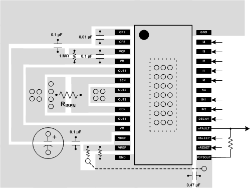
The VM pins should be bypassed to GND using low-ESR ceramic bypass capacitors with a recommended value of 0.1-μF rated for VM. This capacitor should be placed as close to the VM pins as possible with a thick trace or ground plane connection to the device GND pin.

The VM pins must be bypassed to ground using an appropriate bulk capacitor. This component may be an electrolytic and should be located close to the DRV8842-EP.

A low-ESR ceramic capacitor must be placed in between the CPL and CPH pins. TI recommends a value of 0.01-μF rated for VM. Place this component as close to the pins as possible.

A low-ESR ceramic capacitor must be placed in between the VM and VCP pins. TI recommends a value of
0.1-μF rated for 16 V. Place this component as close to the pins as possible. Also, place a 1-MΩ resistor between VCP and VM.

Bypass V3P3 to ground with a ceramic capacitor rated 6.3 V. Place this bypass capacitor as close to the pin as possible.

11.2 Layout Example
layout_ex_LVSCH4.gif