ZHCSCM3 July 2014 DRV8842-EP
PRODUCTION DATA.
9 Application and Implementation
9.1 Application Information
The DRV8842-EP is used in DC motor control. This integrated driver drives up to a 5-A peak with precise winding current control. The motor is controlled through a PWM interface and device faults are reported through the nFAULT pin. The following design is a common application of the DRV8842-EP.
9.2 Typical Application
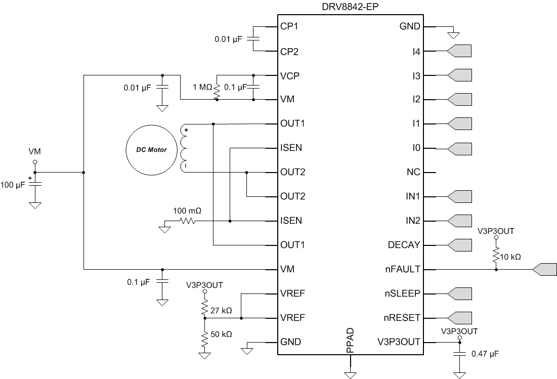
9.2.1 Design Requirements
| Design Parameters | Reference | Example Value |
|---|---|---|
| Supply voltage | VM | 24 V |
| Motor winding resistance | RL | 13.23 Ω |
| Motor winding inductance | IL | 4.03 mH |
| Motor type | BDC | Brushed DC motor |
| Sense resistor | RSENSE | 100 mΩ |
| Full-scale current | IFS | 3.5 A |
9.2.2 Detailed Design Procedure
9.2.2.1 Power Dissipation
Average power dissipation in the DRV8842-EP when running a DC motor can be roughly estimated by Equation 2.

where
- P is the power dissipation of one H-bridge
- RDS(ON) is the resistance of each FET
- IOUT is the RMS output current being applied to each winding
IOUT is equal to the average current drawn by the DC motor. Note that at start-up and fault conditions, this current is much higher than normal running current; also consider the peak currents and their duration. The factor of 2 is due to two FETs conducting winding current (one high side and one low side) at any instant.
The maximum amount of power that can be dissipated in the device depends on ambient temperature and heatsinking.
Note that RDS(ON) increases with temperature, so as the device heats, the power dissipation increases. Take this into consideration when sizing the heatsink.
9.2.2.2 Current Regulation Considerations
For the DRV8842-EP, the set full-scale current (IFS) is the maximum current that can be driven. This quantity depends on the VREF analog voltage and the sense resistor value (RSENSE). The gain of DRV8842-EP is set for 5 V/V. This value can be adjusted from 0% to 100% through the use of the relative current bits I[4:0].

To achieve IFS = 3.5 A with RSENSE of 0.1 Ω, V(VREF) should be 1.75 V, and I[4:0] should be 0x1F.
9.2.2.3 Slow, Fast, and Mixed Decay Modes
The DRV8842-EP supports three different decay modes: slow decay, fast decay, and mixed decay. The current through the motor winding is regulated using a fixed-frequency PWM scheme. This means that after any drive phase, when a motor winding current has hit the current chopping threshold (ITRIP), the DRV8842-EP places the winding in one of the three decay modes until the PWM cycle has expired. After, a new drive phase starts.
The blanking time, TBLANK, defines the minimum drive time for the current chopping. ITRIP is ignored during TBLANK, so the winding current may overshoot the trip level.
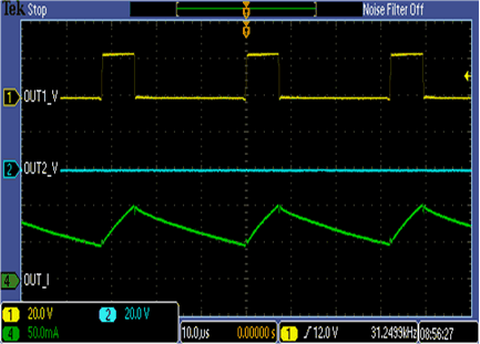
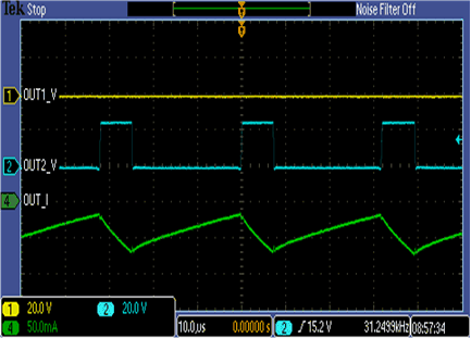
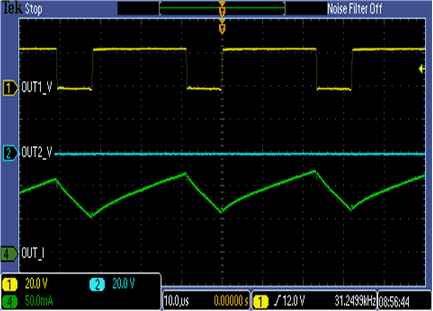
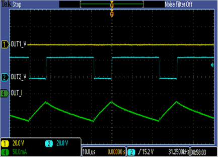
9.2.3 Application Curves
