ZHCSCX5A October   2014  – November 2015 DRV8848

PRODUCTION DATA.  

  1. 特性
  2. 应用
  3. 说明
  4. 修订历史记录
  5. Pin Configuration and Functions
  6. Specifications
    1. 6.1 Absolute Maximum Ratings
    2. 6.2 ESD Ratings
    3. 6.3 Recommended Operating Conditions
    4. 6.4 Thermal Information
    5. 6.5 Electrical Characteristics
    6. 6.6 Timing Requirements
    7. 6.7 Typical Characteristics
  7. Detailed Description
    1. 7.1 Overview
    2. 7.2 Functional Block Diagram
    3. 7.3 Feature Description
      1. 7.3.1 PWM Motor Drivers
      2. 7.3.2 Bridge Control
      3. 7.3.3 Parallel Operation
      4. 7.3.4 Current Regulation
      5. 7.3.5 Current Recirculation and Decay Modes
      6. 7.3.6 Protection Circuits
        1. 7.3.6.1 OCP
        2. 7.3.6.2 TSD
        3. 7.3.6.3 UVLO
    4. 7.4 Device Functional Modes
  8. Application and Implementation
    1. 8.1 Application Information
    2. 8.2 Typical Application
      1. 8.2.1 Design Requirements
      2. 8.2.2 Detailed Design Procedure
        1. 8.2.2.1 Current Regulation
      3. 8.2.3 Application Curves
  9. Power Supply Recommendations
    1. 9.1 Bulk Capacitance Sizing
  10. 10Layout
    1. 10.1 Layout Guidelines
    2. 10.2 Layout Example
  11. 11器件和文档支持
    1. 11.1 社区资源
    2. 11.2 商标
    3. 11.3 静电放电警告
    4. 11.4 Glossary
  12. 12机械、封装和可订购信息

封装选项

机械数据 (封装 | 引脚)
散热焊盘机械数据 (封装 | 引脚)
订购信息

Layout

Layout Guidelines

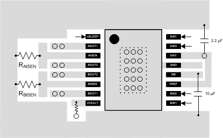
Bypass the VM terminal to GND using a low-ESR ceramic bypass capacitor with a recommended value of 10 μF rated for VM. Place this capacitor as close to the VM pin as possible with a thick trace or ground plane connection to the device GND pin.

Bypass VINT to ground with a ceramic capacitor rated 6.3 V. Place this bypassing capacitor as close to the pin as possible.

Layout Example

DRV8848 layout_ex_LLSEL7.gif Figure 14. Layout Recommendation