ZHCSCX5A October 2014 – November 2015 DRV8848
PRODUCTION DATA.
- 1 特性
- 2 应用
- 3 说明
- 4 修订历史记录
- 5 Pin Configuration and Functions
- 6 Specifications
- 7 Detailed Description
- 8 Application and Implementation
- 9 Power Supply Recommendations
- 10Layout
- 11器件和文档支持
- 12机械、封装和可订购信息
封装选项
机械数据 (封装 | 引脚)
- PWP|16
散热焊盘机械数据 (封装 | 引脚)
- PWP|16
订购信息
8 Application and Implementation
NOTE
Information in the following applications sections is not part of the TI component specification, and TI does not warrant its accuracy or completeness. TI’s customers are responsible for determining suitability of components for their purposes. Customers should validate and test their design implementation to confirm system functionality.
8.1 Application Information
The DRV8848 is used in stepper or brushed DC motor control.
8.2 Typical Application
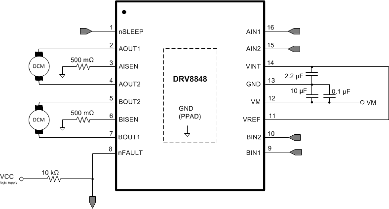
The user can configure the DRV8848 with the following design procedure.
 Figure 10. Typical Application Schematic
8.2.1 Design Requirements
Table 4 gives design input parameters for system design.
Table 4. Design Parameters
| DESIGN PARAMETER | REFERENCE | EXAMPLE VALUE |
|---|---|---|
| Nominal supply voltage | VVM | 12 V |
| Supply voltage range | 4 to 18 V | |
| Motor winding resistance | RL | 3 Ω/phase |
| Motor winding inductance | LL | 330 µH/phase |
| Target chopping current | ICHOP | 500 mA |
| Chopping current reference voltage | VVREF | 3.3 V |
8.2.2 Detailed Design Procedure
8.2.2.1 Current Regulation
The chopping current (ICHOP) is the maximum current driven through either winding. This quantity depends on the sense resistor value (RXISEN).

ICHOP is set by a comparator which compares the voltage across RXISEN to a reference voltage. Note that ICHOP must follow Equation 3 to avoid saturating the motor.

where
- VVM is the motor supply voltage.
- RL is the motor winding resistance.
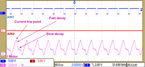
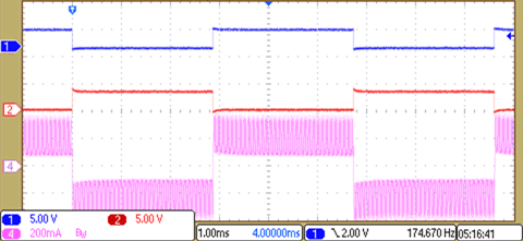
8.2.3 Application Curves

