ZHCSE26B August 2015 – July 2016 DRV8871
PRODUCTION DATA.
7 Detailed Description
7.1 Overview
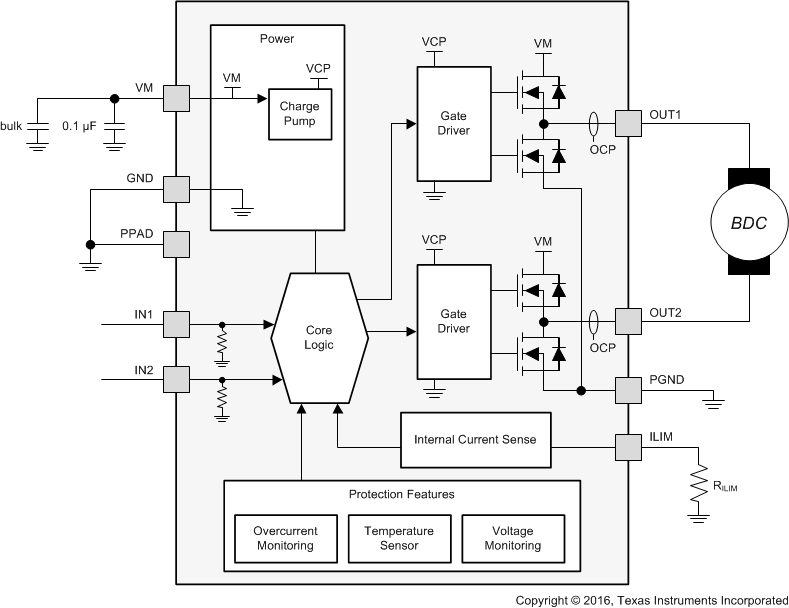
The DRV8871 device is an optimized 8-pin device for driving brushed DC motors with 6.5 to 45 V and up to 3.6-A peak current. The integrated current regulation restricts motor current to a predefined maximum. Two logic inputs control the H-bridge driver, which consists of four N-channel MOSFETs that have a typical Rds(on) of 565 mΩ (including one high-side and one low-side FET). A single power input, VM, serves as both device power and the motor winding bias voltage. The integrated charge pump of the device boosts VM internally and fully enhances the high-side FETs. Motor speed can be controlled with pulse-width modulation, at frequencies between 0 to 100 kHz. The device has an integrated sleep mode that is entered by bringing both inputs low. An assortment of protection features prevent the device from being damaged if a system fault occurs.
7.2 Functional Block Diagram

7.3 Feature Description
7.3.1 Bridge Control
The DRV8871 output consists of four N-channel MOSFETs that are designed to drive high current. They are controlled by the two logic inputs IN1 and IN2, according to Table 1.
Table 1. H-Bridge Control
| IN1 | IN2 | OUT1 | OUT2 | DESCRIPTION |
|---|---|---|---|---|
| 0 | 0 | High-Z | High-Z | Coast; H-bridge disabled to High-Z (sleep entered after 1 ms) |
| 0 | 1 | L | H | Reverse (Current OUT2 → OUT1) |
| 1 | 0 | H | L | Forward (Current OUT1 → OUT2) |
| 1 | 1 | L | L | Brake; low-side slow decay |
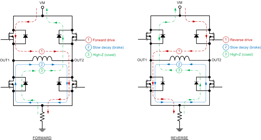
The inputs can be set to static voltages for 100% duty cycle drive, or they can be pulse-width modulated (PWM) for variable motor speed. When using PWM, it typically works best to switch between driving and braking. For example, to drive a motor forward with 50% of its max RPM, IN1 = 1 and IN2 = 0 during the driving period, and IN1 = 1 and IN2 = 1 during the other period. Alternatively, the coast mode (IN1 = 0, IN2 = 0) for fast current decay is also available. The input pins can be powered before VM is applied.
 Figure 4. H-Bridge Current Paths
7.3.2 Sleep Mode
When IN1 and IN2 are both low for time tSLEEP (typically 1 ms), the DRV8871 device enters a low-power sleep mode, where the outputs remain High-Z and the device uses IVMSLEEP (microamps) of current. If the device is powered up while both inputs are low, sleep mode is immediately entered. After IN1 or IN2 are high for at least 5 µs, the device will be operational 50 µs (tON) later.
7.3.3 Current Regulation
The DRV8871 device limits the output current based on a standard resistor attached to pin ILIM, according to this equation:

For example, if RILIM = 32 kΩ, the DRV8871 device limits motor current to 2 A no matter how much load torque is applied. The minimum allowed RILIM is 15 kΩ. System designers should always understand the min and max ITRIP, based on the RILIM resistor component tolerance and the DRV8871 specified VILIM range.
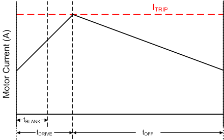
When ITRIP has been reached, the device enforces slow current decay by enabling both low-side FETs, and it does this for time tOFF (typically 25 µs).
 Figure 5. Current Regulation Time Periods
After tOFF has elapsed, the output is re-enabled according to the two inputs INx. The drive time (tDRIVE) until reaching another ITRIP event heavily depends on the VM voltage, the motor’s back-EMF, and the motor’s inductance.
7.3.4 Dead Time
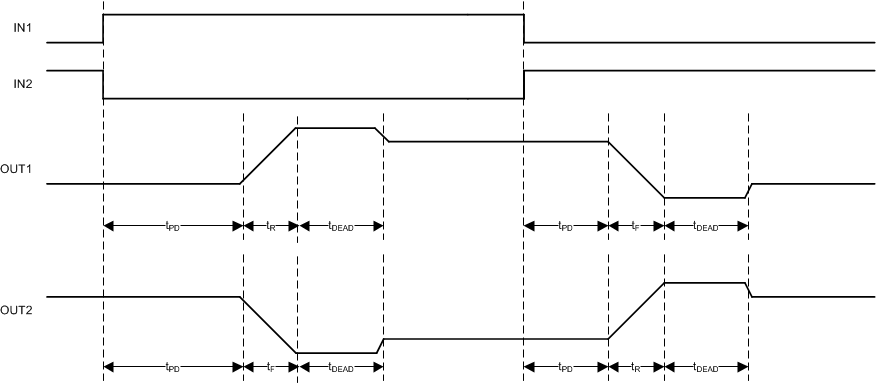
When an output changes from driving high to driving low, or driving low to driving high, dead time is automatically inserted to prevent shoot-through. tDEAD is the time in the middle when the output is High-Z. If the output pin is measured during tDEAD, the voltage will depend on the direction of current. If current is leaving the pin, the voltage will be a diode drop below ground. If current is entering the pin, the voltage will be a diode drop above VM. This diode is the body diode of the high-side or low-side FET.
 Figure 6. Propagation Delay Time
7.3.5 Protection Circuits
The DRV8871 device is fully protected against VM undervoltage, overcurrent, and overtemperature events.
7.3.5.1 VM Undervoltage Lockout (UVLO)
If at any time the voltage on the VM pin falls below the undervoltage lockout threshold voltage, all FETs in the H-bridge will be disabled. Operation will resume when VM rises above the UVLO threshold.
7.3.5.2 Overcurrent Protection (OCP)
If the output current exceeds the OCP threshold IOCP for longer than tOCP, all FETs in the H-bridge are disabled for a duration of tRETRY. After that, the H-bridge will be re-enabled according to the state of the INx pins. If the overcurrent fault is still present, the cycle repeats; otherwise normal device operation resumes.
7.3.5.3 Thermal Shutdown (TSD)
If the die temperature exceeds safe limits, all FETs in the H-bridge will be disabled. After the die temperature has fallen to a safe level, operation automatically resumes.
Table 2. Protection Functionality
| FAULT | CONDITION | H-BRIDGE STATUS | RECOVERY |
|---|---|---|---|
| VM undervoltage lockout (UVLO) | VM < VUVLO | Disabled | VM > VUVLO |
| Overcurrent (OCP) | IOUT > IOCP | Disabled | tRETRY |
| Thermal Shutdown (TSD) | TJ > 150°C | Disabled | TJ < TSD – T HYS |
7.4 Device Functional Modes
The DRV8871 device can be used in multiple ways to drive a brushed DC motor.
7.4.1 PWM With Current Regulation
This scheme uses all of the device capabilities. ITRIP is set above the normal operating current, and high enough to achieve an adequate spin-up time, but low enough to constrain current to a desired level. Motor speed is controlled by the duty cycle of one of the inputs, while the other input is static. Brake/slow decay is typically used during the off-time.
7.4.2 PWM Without Current Regulation
If current regulation is not needed, a 15-kΩ to 18-kΩ resistor should be used on pin ILIM. This mode provides the highest possible peak current: up to 3.6 A for a few hundred milliseconds (depending on PCB characteristics and the ambient temperature). If current exceeds 3.6 A, the device might reach overcurrent protection (OCP) or overtemperature shutdown (TSD). If that happens, the device disables and protects itself for about 3 ms (tRETRY) and then resumes normal operation.
7.4.3 Static Inputs With Current Regulation
IN1 and IN2 can be set high and low for 100% duty cycle drive, and ITRIP can be used to control the current, speed, and torque capability of the motor.
7.4.4 VM Control
In some systems it is desirable to vary VM as a means of changing motor speed. See Motor Voltage for more information.