ZHCSE40C August 2015 – July 2016 DRV8872
PRODUCTION DATA.
6 Specifications
6.1 Absolute Maximum Ratings
over operating free-air temperature range (unless otherwise noted)(1)| MIN | MAX | UNIT | |
|---|---|---|---|
| Power supply voltage (VM) | –0.3 | 50 | V |
| Logic input voltage (IN1, IN2) | –0.3 | 7 | V |
| Fault pin (nFAULT) | –0.3 | 6 | V |
| Continuous phase node pin voltage (OUT1, OUT2) | –0.7 | VM + 0.7 | V |
| Current sense input pin voltage (ISEN)(2) | –0.5 | 1 | V |
| Output current (100% duty cycle) | 0 | 3.5 | A |
| Operating junction temperature, TJ | –40 | 150 | °C |
| Storage temperature, Tstg | –65 | 150 | °C |
(1) Stresses beyond those listed under Absolute Maximum Ratings may cause permanent damage to the device. These are stress ratings only, which do not imply functional operation of the device at these or any other conditions beyond those indicated under Recommended Operating Conditions. Exposure to absolute-maximum-rated conditions for extended periods may affect device reliability.
(2) Transients of ±1 V for less than 25 ns are acceptable
6.2 ESD Ratings
| VALUE | UNIT | |||
|---|---|---|---|---|
| V(ESD) | Electrostatic discharge | Human-body model (HBM), per ANSI/ESDA/JEDEC JS-001(1) | ±6000 | V |
| Charged-device model (CDM), per JEDEC specification JESD22-C101(2) | ±750 | |||
(1) JEDEC document JEP155 states that 500-V HBM allows safe manufacturing with a standard ESD control process.
(2) JEDEC document JEP157 states that 250-V CDM allows safe manufacturing with a standard ESD control process.
6.3 Recommended Operating Conditions
over operating free-air temperature range (unless otherwise noted)| MIN | NOM | MAX | UNIT | ||
|---|---|---|---|---|---|
| VM | Power supply voltage | 6.5 | 45 | V | |
| VI | Logic input voltage (IN1, IN2) | 0 | 5.5 | V | |
| fPWM | Logic input PWM frequency (IN1, IN2) | 0 | 200(2) | kHz | |
| Ipeak | Peak output current(1) | 0 | 3.6 | A | |
| TA | Operating ambient temperature | –40 | 125 | °C | |
(1) Power dissipation and thermal limits must be observed
(2) The voltages applied to the inputs should have at least 800 ns of pulse width to ensure detection. Typical devices require at least 400 ns. If the PWM frequency is 200 kHz, the usable duty cycle range is 16% to 84%
6.4 Thermal Information
| THERMAL METRIC(1) | DRV8872 | UNIT | |
|---|---|---|---|
| DDA (HSOP) | |||
| 8 PINS | |||
| RθJA | Junction-to-ambient thermal resistance | 41.1 | °C/W |
| RθJC(top) | Junction-to-case (top) thermal resistance | 53.1 | °C/W |
| RθJB | Junction-to-board thermal resistance | 23.1 | °C/W |
| ψJT | Junction-to-top characterization parameter | 8.2 | °C/W |
| ψJB | Junction-to-board characterization parameter | 23 | °C/W |
| RθJC(bot) | Junction-to-case (bottom) thermal resistance | 2.7 | °C/W |
(1) For more information about traditional and new thermal metrics, see the Semiconductor and IC Package Thermal Metrics application report.
6.5 Electrical Characteristics
TA = 25°C, over recommended operating conditions (unless otherwise noted)| PARAMETER | TEST CONDITIONS | MIN | TYP | MAX | UNIT | |
|---|---|---|---|---|---|---|
| POWER SUPPLY (VM) | ||||||
| VM | VM operating voltage | 6.5 | 45 | V | ||
| IVM | VM operating supply current | VM = 12 V | 3 | 10 | mA | |
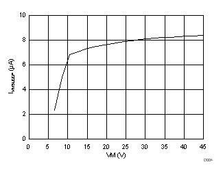
| IVMSLEEP | VM sleep current | VM = 12 V | 10 | µA | ||
| tON | Turn-on time(1) | VM > VUVLO with IN1 or IN2 high | 40 | 50 | µs | |
| LOGIC-LEVEL INPUTS (IN1, IN2) | ||||||
| VIL | Input logic low voltage | 0.5 | V | |||
| VIH | Input logic high voltage | 1.5 | V | |||
| VHYS | Input logic hysteresis | 0.5 | V | |||
| IIL | Input logic low current | VIN = 0 V | –1 | 1 | μA | |
| IIH | Input logic high current | VIN = 3.3 V | 33 | 100 | μA | |
| RPD | Pulldown resistance | To GND | 100 | kΩ | ||
| tPD | Propagation delay | INx to OUTx change (see Figure 6) | 0.7 | 1 | μs | |
| tsleep | Time to sleep | Inputs low to sleep | 1 | 1.5 | ms | |
| MOTOR DRIVER OUTPUTS (OUT1, OUT2) | ||||||
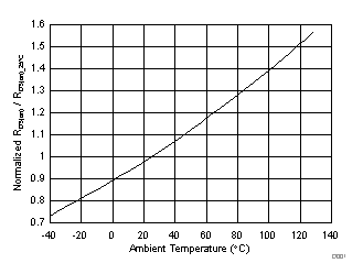
| RDS(ON) | High-side FET on resistance | VM = 24 V, I = 1 A, fPWM = 25 kHz | 307 | 360 | mΩ | |
| RDS(ON) | Low-side FET on resistance | VM = 24 V, I = 1 A, fPWM = 25 kHz | 258 | 320 | mΩ | |
| tDEAD | Output dead time | 220 | ns | |||
| Vd | Body diode forward voltage | IOUT = 1 A | 0.8 | 1 | V | |
| CURRENT REGULATION | ||||||
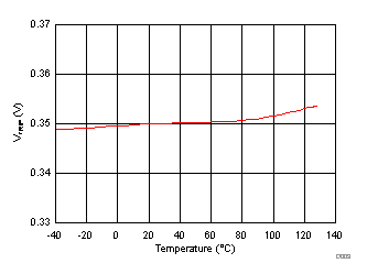
| VTRIP | ISEN voltage for current chopping | 0.32 | 0.35 | 0.38 | V | |
| tOFF | PWM off-time | 25 | μs | |||
| tBLANK | PWM blanking time | 2 | µs | |||
| PROTECTION CIRCUITS | ||||||
| VUVLO | VM undervoltage lockout | VM falls until UVLO triggers | 6.1 | 6.4 | V | |
| VM rises until operation recovers | 6.3 | 6.5 | ||||
| VUV,HYS | VM undervoltage hysteresis | Rising to falling threshold | 100 | 180 | mV | |
| IOCP | Overcurrent protection trip level | 3.7 | 4.5 | 6.4 | A | |
| tOCP | Overcurrent deglitch time | 1.5 | μs | |||
| tRETRY | Overcurrent retry time | 3 | ms | |||
| TSD | Thermal shutdown temperature | 150 | 175 | °C | ||
| THYS | Thermal shutdown hysteresis | 40 | °C | |||
| nFAULT OPEN DRAIN OUTPUT | ||||||
| VOL | Output low voltage | IO = 5 mA | 0.5 | V | ||
| IOH | Output high leakage current | VO = 3.3 V | 1 | µA | ||
(1) tON applies when the device initially powers up, and when it exits sleep mode.
6.6 Typical Characteristics


