ZHCSIO5B October   2017  – January 2021 DRV8873-Q1

PRODUCTION DATA  

  1. 特性
  2. 应用
  3. 说明
  4. Revision History
  5. Pin Configuration and Functions
    1.     Pin Functions
  6. Specifications
    1. 6.1 Absolute Maximum Ratings
    2. 6.2 ESD Ratings
    3. 6.3 Recommended Operating Conditions
    4. 6.4 Thermal Information
    5. 6.5 Electrical Characteristics
    6. 6.6 SPI Timing Requirements
    7. 6.7 Typical Characteristics
  7. Detailed Description
    1. 7.1 Overview
    2. 7.2 Functional Block Diagram
    3. 7.3 Feature Description
      1. 7.3.1 Bridge Control
        1. 7.3.1.1 Control Modes
        2. 7.3.1.2 Half-Bridge Operation
        3. 7.3.1.3 22
        4. 7.3.1.4 Internal Current Sense and Current Regulation
        5. 7.3.1.5 Slew-Rate Control
        6. 7.3.1.6 Dead Time
        7. 7.3.1.7 Propagation Delay
        8. 7.3.1.8 nFAULT Pin
        9. 7.3.1.9 nSLEEP as SDO Reference
      2. 7.3.2 Motor Driver Protection Circuits
        1. 7.3.2.1 VM Undervoltage Lockout (UVLO)
        2. 7.3.2.2 VCP Undervoltage Lockout (CPUV)
        3. 7.3.2.3 Overcurrent Protection (OCP)
          1. 7.3.2.3.1 Latched Shutdown (OCP_MODE = 00b)
          2. 7.3.2.3.2 Automatic Retry (OCP_MODE = 01b)
          3. 7.3.2.3.3 Report Only (OCP_MODE = 10b)
          4. 7.3.2.3.4 Disabled (OCP_MODE = 11b)
        4. 7.3.2.4 Open-Load Detection (OLD)
          1. 7.3.2.4.1 Open-Load Detection in Passive Mode (OLP)
          2. 7.3.2.4.2 Open-Load Detection in Active Mode (OLA)
        5. 7.3.2.5 Thermal Shutdown (TSD)
          1. 7.3.2.5.1 Latched Shutdown (TSD_MODE = 0b)
          2. 7.3.2.5.2 Automatic Recovery (TSD_MODE = 1b)
        6. 7.3.2.6 Thermal Warning (OTW)
      3. 7.3.3 Hardware Interface
        1. 7.3.3.1 MODE (Tri-Level Input)
        2. 7.3.3.2 Slew Rate
    4. 7.4 Device Functional Modes
      1. 7.4.1 Motor Driver Functional Modes
        1. 7.4.1.1 Sleep Mode (nSLEEP = 0)
        2. 7.4.1.2 Disable Mode (nSLEEP = 1, DISABLE = 1)
        3. 7.4.1.3 Operating Mode (nSLEEP = 1, DISABLE = 0)
        4. 7.4.1.4 nSLEEP Reset Pulse
    5. 7.5 Programming
      1. 7.5.1 Serial Peripheral Interface (SPI) Communication
        1. 7.5.1.1 SPI Format
        2. 7.5.1.2 SPI for a Single Slave Device
        3. 7.5.1.3 SPI for Multiple Slave Devices in Parallel Configuration
        4. 7.5.1.4 SPI for Multiple Slave Devices in Daisy Chain Configuration
    6. 7.6 Register Maps
  8. Application and Implementation
    1. 8.1 Application Information
    2. 8.2 Typical Application
      1. 8.2.1 Design Requirements
        1. 8.2.1.1 Motor Voltage
        2. 8.2.1.2 Drive Current and Power Dissipation
        3. 8.2.1.3 Sense Resistor
      2. 8.2.2 Detailed Design Procedure
        1. 8.2.2.1 Thermal Considerations
        2. 8.2.2.2 Heatsinking
      3. 8.2.3 Application Curves
  9. Power Supply Recommendations
    1. 9.1 Bulk Capacitance Sizing
  10. 10Layout
    1. 10.1 Layout Guidelines
    2. 10.2 Layout Example
  11. 11Device and Documentation Support
    1. 11.1 Documentation Support
      1. 11.1.1 Related Documentation
    2. 11.2 Receiving Notification of Documentation Updates
    3. 11.3 支持资源
    4. 11.4 Trademarks
    5. 11.5 静电放电警告
    6. 11.6 术语表
  12. 12Mechanical, Packaging, and Orderable Information

封装选项

机械数据 (封装 | 引脚)
散热焊盘机械数据 (封装 | 引脚)
订购信息

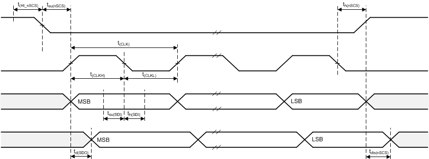
SPI Timing Requirements

MINNOMMAXUNIT
t(READY)SPI ready, VM > V(UVLO)1ms
t(CLK)SCLK minimum period100ns
t(CLKH)SCLK minimum high time50ns
t(CLKL)SCLK minimum low time50ns
tsu(SDI)SDI input setup time20ns
th(SDI)SDI input hold time30ns
td(SDO)SDO output delay time, SCLK high to SDO valid, CL = 20 pF30ns
tsu(nSCS)nSCS input setup time50ns
th(nSCS)nSCS input hold time50ns
t(HI_nSCS)nSCS minimum high time before active low500ns
tdis(nSCS)nSCS disable time, nSCS high to SDO high impedance10ns
GUID-5897548B-4068-4291-959D-3130ED7314F9-low.gifFigure 6-1 SPI Slave-Mode Timing Definition