SLVSET1 August   2018 DRV8873

PRODUCTION DATA.  

  1. Features
  2. Applications
  3. Description
    1.     Simplified Schematic
  4. Revision History
  5. Pin Configuration and Functions
    1.     Pin Functions
  6. Specifications
    1. 6.1 Absolute Maximum Ratings
    2. 6.2 ESD Ratings
    3. 6.3 Recommended Operating Conditions
    4. 6.4 Thermal Information
    5. 6.5 Electrical Characteristics
    6. 6.6 SPI Timing Requirements
    7. 6.7 Typical Characteristics
  7. Detailed Description
    1. 7.1 Overview
    2. 7.2 Functional Block Diagram
    3. 7.3 Feature Description
      1. 7.3.1 Bridge Control
        1. 7.3.1.1 Control Modes
        2. 7.3.1.2 Half-Bridge Operation
        3. 7.3.1.3 Internal Current Sense and Current Regulation
        4. 7.3.1.4 Slew-Rate Control
        5. 7.3.1.5 Dead Time
        6. 7.3.1.6 Propagation Delay
        7. 7.3.1.7 nFAULT Pin
        8. 7.3.1.8 nSLEEP as SDO Reference
      2. 7.3.2 Motor Driver Protection Circuits
        1. 7.3.2.1 VM Undervoltage Lockout (UVLO)
        2. 7.3.2.2 VCP Undervoltage Lockout (CPUV)
        3. 7.3.2.3 Overcurrent Protection (OCP)
          1. 7.3.2.3.1 Latched Shutdown (OCP_MODE = 00b)
          2. 7.3.2.3.2 Automatic Retry (OCP_MODE = 01b)
          3. 7.3.2.3.3 Report Only (OCP_MODE = 10b)
          4. 7.3.2.3.4 Disabled (OCP_MODE = 11b)
        4. 7.3.2.4 Open-Load Detection (OLD)
          1. 7.3.2.4.1 Open-Load Detection in Passive Mode (OLP)
          2. 7.3.2.4.2 Open-Load Detection in Active Mode (OLA)
        5. 7.3.2.5 Thermal Shutdown (TSD)
          1. 7.3.2.5.1 Latched Shutdown (TSD_MODE = 0b)
          2. 7.3.2.5.2 Automatic Recovery (TSD_MODE = 1b)
        6. 7.3.2.6 Thermal Warning (OTW)
      3. 7.3.3 Hardware Interface
        1. 7.3.3.1 MODE (Tri-Level Input)
        2. 7.3.3.2 Slew Rate
    4. 7.4 Device Functional Modes
      1. 7.4.1 Motor Driver Functional Modes
        1. 7.4.1.1 Sleep Mode (nSLEEP = 0)
        2. 7.4.1.2 Disable Mode (nSLEEP = 1, DISABLE = 1)
        3. 7.4.1.3 Operating Mode (nSLEEP = 1, DISABLE = 0)
        4. 7.4.1.4 nSLEEP Reset Pulse
    5. 7.5 Programming
      1. 7.5.1 Serial Peripheral Interface (SPI) Communication
        1. 7.5.1.1 SPI Format
        2. 7.5.1.2 SPI for a Single Slave Device
        3. 7.5.1.3 SPI for Multiple Slave Devices in Parallel Configuration
        4. 7.5.1.4 SPI for Multiple Slave Devices in Daisy Chain Configuration
    6. 7.6 Register Maps
      1. 7.6.1 Status Registers
        1. 7.6.1.1 FAULT Status Register Name (address = 0x00)
          1. Table 21. FAULT Status Register Field Descriptions
        2. 7.6.1.2 DIAG Status Register Name (address = 0x01)
          1. Table 22. DIAG Status Register Field Descriptions
      2. 7.6.2 Control Registers
        1. 7.6.2.1 IC1 Control Register (address = 0x02)
          1. Table 24. IC1 Control Register Field Descriptions
        2. 7.6.2.2 IC2 Control Register (address = 0x03)
          1. Table 25. IC2 Control Register Field Descriptions
        3. 7.6.2.3 IC3 Control Register (address = 0x04)
          1. Table 26. IC3 Control Register Field Descriptions
        4. 7.6.2.4 IC4 Control Register (address = 0x05)
          1. Table 27. IC4 Control Register Field Descriptions
  8. Application and Implementation
    1. 8.1 Application Information
    2. 8.2 Typical Application
      1. 8.2.1 Design Requirements
        1. 8.2.1.1 Motor Voltage
        2. 8.2.1.2 Drive Current and Power Dissipation
        3. 8.2.1.3 Sense Resistor
      2. 8.2.2 Detailed Design Procedure
        1. 8.2.2.1 Thermal Considerations
        2. 8.2.2.2 Heatsinking
      3. 8.2.3 Application Curves
  9. Power Supply Recommendations
    1. 9.1 Bulk Capacitance Sizing
  10. 10Layout
    1. 10.1 Layout Guidelines
    2. 10.2 Layout Example
  11. 11Device and Documentation Support
    1. 11.1 Documentation Support
      1. 11.1.1 Related Documentation
    2. 11.2 Receiving Notification of Documentation Updates
    3. 11.3 Community Resources
    4. 11.4 Trademarks
    5. 11.5 Electrostatic Discharge Caution
    6. 11.6 Glossary
  12. 12Mechanical, Packaging, and Orderable Information
    1. 12.1 Package Option Addendum
      1. 12.1.1 Packaging Information
      2. 12.1.2 Tape and Reel Information

封装选项

机械数据 (封装 | 引脚)
散热焊盘机械数据 (封装 | 引脚)
订购信息

Description

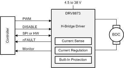
The DRV8873 device is an integrated driver IC for driving a brushed DC motor in industrial applications. Two logic inputs control the H-bridge driver, which consists of four N-channel MOSFETs that drive motors bi-directionally with up to 10-A peak current. The device operates from a single power supply and supports a wide input supply range from 4.5 V to 38 V.

A PH/EN or PWM interface allows simple interfacing to controller circuits. Alternatively, independent half-bridge control is available to drive two solenoid loads.

A current mirror allows the controller to monitor the load current. This mirror approximates the current through the high-side FETs, and does not require a high-power resistor for sensing the current.

A low-power sleep mode is provided to achieve very-low quiescent current draw by shutting down much of the internal circuitry. Internal protection functions are provided for undervoltage lockout, charge pump faults, overcurrent protection, short-circuit protection, open-load detection, and overtemperature. Fault conditions are indicated on an nFAULT pin and through the SPI registers.

Device Information(1)

PART NUMBER PACKAGE BODY SIZE (NOM)
DRV8873 HTSSOP (24) 7.70 mm × 4.40 mm
  1. For all available packages, see the orderable addendum at the end of the data sheet.

Simplified Schematic
DRV8873 drv8873-simplified-schematic.gif