SLVSET1 August 2018 DRV8873
PRODUCTION DATA.
- 1 Features
- 2 Applications
- 3 Description
- 4 Revision History
- 5 Pin Configuration and Functions
- 6 Specifications
-
7 Detailed Description
- 7.1 Overview
- 7.2 Functional Block Diagram
- 7.3 Feature Description
- 7.4 Device Functional Modes
- 7.5 Programming
- 7.6 Register Maps
- 8 Application and Implementation
- 9 Power Supply Recommendations
- 10Layout
- 11Device and Documentation Support
- 12Mechanical, Packaging, and Orderable Information
7.3.1.3 Internal Current Sense and Current Regulation
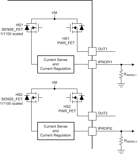
The IPROPI pin outputs an analog current that is proportional to the current flowing in the H-bridge. The output current is typically 1/1100 of the current in both high-side FETs. The IPROPI pin is derived from the current through either of the high-side FETs. Because of this, the IPROPI pin does not represent the half bridge current when operating in a fast decay mode or low-side slow decay mode. The IPROPI pin represents the H-bridge current under forward drive, reverse drive, and high-side slow decay. The IPROPI output is delayed by approximately 2 µs for the fastest slew-rate setting (43.2 V/µs) after the high-side FET is switched on.
 Figure 12. Current-Sense Block Diagram
 The selection of the external resistor should be such that the voltage on the IPROPI pin is less than 5 V. Therefore the resistor must be sized less than this value based on Equation 1. The range of current that can be monitored is from 100 mA to 10 A assuming the selected external resistor meets the calculated value from Equation 1. If the current exceeds 10 A, the device could reach overcurrent protection (OCP) or overtemperature shutdown (TSD). If OCP occurs, the device disables the internal MOSFETs and protects itself (for the hardware version of the device) or based on the OCP_MODE setting (for the SPI version of the device). For guidelines on selecting a sense resistor, see the Sense Resistor section.
where
- k is the current mirror scaling factor, which is typically 1100.
- IO is the maximum drive current to be monitored.
NOTE
Texas Instruments recommends the load current not exceed 8 A during normal operation. If slew rate setting of 2.6 V/µs (SR = 111b) is used when the load current is about 8 A, choose TOFF to be either 40 µs or 60 µs.
The SPI version of the device limits the output current based on the trip level set in the SPI registers. In the hardware version of the device, the current trip limit is set to 6.5 A. The current regulation feature is enabled by default on both the outputs (OUT1 and OUT2). To disable current regulation in the hardware version of the device, the nITRIP pin must be connected to DVDD. To disable current regulation in the SPI version of the device, the DIS_ITRIP bits in the IC4 Control register must be written to. The bit settings are:
- 01b to disable current regulation only on the OUT1 pin
- 10b to disable current regulation only on the OUT2 pin
- 11b to disable current regulation on both the OUT1 and OUT2 pins
Table 8. Control Regulation Threshold
| PARAMETER | ITRIP_LVL BIT | MIN | TYP | MAX | UNIT | |
|---|---|---|---|---|---|---|
| ITRIP | Current limit threshold | ITRIP_LVL = 00b | 3.4 | 4 | 4.6 | A |
| ITRIP_LVL = 01b | 4.6 | 5.4 | 6.2 | A | ||
| ITRIP_LVL = 10b | 5.5 | 6.5 | 7.5 | A | ||
| ITRIP_LVL = 11b | 6 | 7 | 8 | A | ||
When the ITRIP current has been reached, the device enforces slow current decay by enabling both the high-side FETs for a time of tOFF . In the hardware version of the device, the tOFF time is 40 µs. The tOFF time is selectable through SPI in the SPI version of the device, as shown in Table 9. The default setting is 01b (tOFF = 40 µs).
Table 9. PWM Off Time Settings
| PARAMETER | TOFF BIT | tOFF DURATION | UNIT | |
|---|---|---|---|---|
| tOFF | PWM off time | TOFF = 00b | 20 | µs |
| TOFF = 01b | 40 | µs | ||
| TOFF = 10b | 60 | µs | ||
| TOFF = 11b | 80 | µs | ||
 Figure 13. Current Regulation Time Periods
 When the tOFF time has elapsed and the current level falls below the current regulation (ITRIP) level, the output is re-enabled according to the inputs. If, after the tOFF time has elapsed the current is still higher than the ITRIP level, the device enforces another tOFF time period of the same duration.
The drive time (tDRIVE) occurs until another ITRIP event is reached and depends heavily on the VM voltage, the back-EMF of the motor, and the inductance of the motor. During the tDRIVE time, the current-sense regulator does not enforce the ITRIP limit until the tBLANK time has elapsed. While in current regulation, the inputs can be toggled to drive the load in the opposite direction to decay the current faster. For example, if the load was in forward drive prior to entering current regulation it can only go into reverse drive when the driver enforces current regulation.
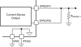
The IPROPI1 pin represents the current flowing through the HS1 MOSFET of half-bridge 1. The IPROPI2 pin represents the current flowing through the HS2 MOSFET of half-bridge 2. To measure current with one sense resistor, the IPROPI1 and IPROPI2 pins must be connected together with the RSENSE resistor as shown in Figure 14. In this configuration, the current-sense output is proportional to the sum of the currents flowing through the both high-side FETs.
 Figure 14. Current Sense Output