SLVSET1 August 2018 DRV8873
PRODUCTION DATA.
- 1 Features
- 2 Applications
- 3 Description
- 4 Revision History
- 5 Pin Configuration and Functions
- 6 Specifications
-
7 Detailed Description
- 7.1 Overview
- 7.2 Functional Block Diagram
- 7.3 Feature Description
- 7.4 Device Functional Modes
- 7.5 Programming
- 7.6 Register Maps
- 8 Application and Implementation
- 9 Power Supply Recommendations
- 10Layout
- 11Device and Documentation Support
- 12Mechanical, Packaging, and Orderable Information
7.3.2.4.1 Open-Load Detection in Passive Mode (OLP)
The open-load passive diagnostic (OLP) is different for the hardware and SPI version of the device. The OLP test is available in all three modes of operation (PN/EN, PWM, and independent half-bridge). When the open-load test is running, the internal power MOSFETs are disabled.
For the hardware version of the device, the OLP test is performed at power-up or after exiting sleep mode if the nOL pin is left as a no connect pin (or tied to GND). If the nOL pin is tied to the DVDD pin (or an external 5-V rail), the OLP test is not performed by the device.
For the SPI version of the device, the OLP test is performed when commanded. The following sequence shows how to perform the OLP test directly after the device powers up:
- Power up the device (DISABLE pin high).
- Select the mode through SPI.
- Wait for the t(DISABLE) time to expire.
- Write 1b to the EN_OL bit in the IC1 register.
- Perform the OLP test.
- If an open load (OL) is detected, the nFAULT pin is driven low, the FAULT and OLx bits are latched high. When the OL condition is removed, a clear faults command must be issued by the MCU either through the CLR_FLT bit or an nSLEEP reset pulse which resets the OLx register bit.
- If an OL condition is not detected, the EN_OL bits return to the default setting (0b) after the td(OL) time expires.
- Set the DISABLE pin low so that the device drives the motor or load based on the input signals.
If an open-load diagnostic is performed at any other time, the following sequence must be followed:
- Set the pin DISABLE high (to disable the half bridge outputs).
- Wait for the t(DISABLE) time to expire.
- Write 1b to the EN_OL bit in the IC1 register.
- Perform the OLP test.
- If an OL condition is detected, the nFAULT pin is driven low, and the FAULT and OLx bits are latched high. When the OL condition is removed, a clear faults command must be issued by the MCU either through the CLR_FLT bit or an nSLEEP reset pulse which resets the OLx register bits.
- If an OL condition is not detected, the EN_OL bits return to the default setting (0b) after the td(OL) time expires.
- Set the DISABLE pin low so that the device drives the motor or load based on the input signals.
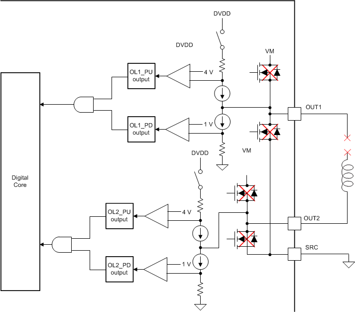
 Figure 19. Open-Load Detection Circuit
 The EN_OL register maintains the written command until the diagnostic is complete. The signal on the DISABLE pin must remain high for the entire duration of the test. While the OLP test is running, if the DISABLE pin goes low, the OLP test is aborted to resume normal operation and no fault is reported. The OLP test is not performed if the motor is energized.
The OLD test checks for a high-impedance connection on the OUTx pins. The diagnostic runs in two steps. First the pullup current source is enabled. If a load is connected, the current passes through the pullup resistor and the OLx_PU comparator output remains low. If an OL condition exists, the current through the pullup resistor goes to 0 A and the OLx_PU comparator trips high. Second the pulldown current source is enabled. In the same way, the OLx_PD comparator output either remains low to indicate that a load is connected, or trips high to indicate an OL condition.
If both the OLx_PU and OLx_PD comparators report an OL condition, the OLx bit in the SPI register latches high and the nFAULT line goes low to indicate an OL fault. When the OL condition is removed, a clear faults command must be issued by the MCU either through the CLR_FLT bit or an nSLEEP reset pulse which resets the OL1 and OL2 register bits. The charge pump remains active during this fault condition.