SLVSF66A August 2019 – December 2019 DRV8874
PRODUCTION DATA.
- 1 Features
- 2 Applications
- 3 Description
- 4 Revision History
- 5 Pin Configuration and Functions
- 6 Specifications
- 7 Detailed Description
- 8 Application and Implementation
- 9 Power Supply Recommendations
- 10Layout
- 11Device and Documentation Support
- 12Mechanical, Packaging, and Orderable Information
7.3.3.2.2 Cycle-By-Cycle Current Chopping
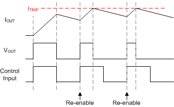
In cycle-by-cycle mode, the H-bridge enters a brake, low-side slow decay state (both low-side MOSFETs ON) after IOUT exceeds ITRIP until the next control input edge on the EN/IN1 or PH/IN2 pins. This allows for additional control of the current chopping scheme by the external controller. This is shown in Figure 13. Cycle-by-cycle mode will not support 100% duty cycle current regulation as a new control input edge is required to reset the outputs after the brake, low-side slow decay state has been entered.
 Figure 13. Cycle-By-Cycle Current Regulation
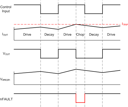
 In cycle-by-cycle mode, the device will also indicate whenever the H-bridge enters internal current chopping by pulling the nFAULT pin low. This can be used to determine when the device outputs will differ from the control inputs or the load has reached the ITRIP threshold. This is shown in Figure 14. nFAULT will be released whenever the next control input edge is received by the device and the outputs are reset.
 Figure 14. Cycle-By-Cycle Current Regulation Where nFAULT Acts as Current Chopping Indicator
 No device functionality is affected when the nFAULT pin is pulled low for the current chopping indicator. The nFAULT pin is only used as an indicator and the device will continue normal operation. To distinguish a device fault (outlined in the Protection Circuits section) from the current chopping indicator, the nFAULT pin can be compared with the control inputs. The current chopping indicator can only assert when the control inputs are commanding a forward or reverse drive state (Figure 10). If the nFAULT pin behavior deviates from the operation shown in Figure 14 then one of the following situations has occurred:
- If a device fault has occurred, then the nFAULT pin pulls low to indicate a fault condition rather than current chopping. Depending on the device fault, nFAULT may remain low even when the control inputs are commanding the high-Z or slow-decay states.
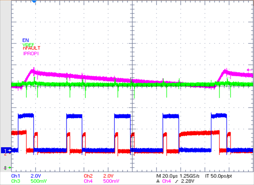
- When the control inputs transition from drive to slow decay, the nFAULT pin will go high for tBLKthen be pulled low again if IOUT > ITRIP. This may be caused by a PWM frequency or duty cycle on the control inputs with a off-time that is too short for the IOUT current to decay below the ITRIP threshold. Figure 15 shows an example of this condition. The condition IOUT > ITRIP can be viewed on an oscilloscope as VIPROPI > VREF.

| Chan. 1 = EN | Chan. 2 = nFAULT | ||
| Chan. 3 = VREF | Chan. 4 = IPROPI |