ZHCSDY9A June 2015 – July 2015 DRV8881
PRODUCTION DATA.
- 1 特性
- 2 应用
- 3 说明
- 4 修订历史记录
- 5 Pin Configuration and Functions
- 6 Specifications
-
7 Detailed Description
- 7.1 Overview
- 7.2 Functional Block Diagrams
- 7.3
Feature Description
- 7.3.1 Motor Driver Current Ratings
- 7.3.2 PWM Motor Drivers
- 7.3.3 Bridge Control
- 7.3.4 Current Regulation
- 7.3.5 Decay Modes
- 7.3.6 AutoTune
- 7.3.7 Adaptive Blanking Time
- 7.3.8 Parallel Mode
- 7.3.9 Charge Pump
- 7.3.10 LDO Voltage Regulator
- 7.3.11 Logic and Tri-Level Pin Diagrams
- 7.3.12 Protection Circuits
- 7.4 Device Functional Modes
- 8 Application and Implementation
- 9 Power Supply Recommendations
- 10Layout
- 11器件和文档支持
- 12机械、封装和可订购信息
封装选项
机械数据 (封装 | 引脚)
散热焊盘机械数据 (封装 | 引脚)
订购信息
10 Layout
10.1 Layout Guidelines
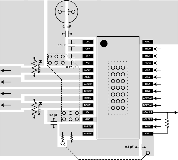
Each VM terminal must be bypassed to GND using a low-ESR ceramic bypass capacitors with recommended values of 0.1 μF rated for VM. These capacitors should be placed as close to the VM pins as possible with a thick trace or ground plane connection to the device GND pin.
The VM pin must be bypassed to ground using a bulk capacitor rated for VM. This component may be an electrolytic.
A low-ESR ceramic capacitor must be placed in between the CPL and CPH pins. A value of 0.1 μF rated for VM is recommended. Place this component as close to the pins as possible.
A low-ESR ceramic capacitor must be placed in between the VM and VCP pins. A value of 0.47 μF rated for 16 V is recommended. Place this component as close to the pins as possible.
Bypass V3P3 to ground with a ceramic capacitor rated 6.3 V. Place this bypassing capacitor as close to the pin as possible.
The current sense resistors should be placed as close as possible to the device pins in order to minimize trace inductance between the pin and resistor.
10.2 Layout Example
 Figure 33. Layout Recommendation