ZHCSDY9A June 2015 – July 2015 DRV8881
PRODUCTION DATA.
- 1 特性
- 2 应用
- 3 说明
- 4 修订历史记录
- 5 Pin Configuration and Functions
- 6 Specifications
-
7 Detailed Description
- 7.1 Overview
- 7.2 Functional Block Diagrams
- 7.3
Feature Description
- 7.3.1 Motor Driver Current Ratings
- 7.3.2 PWM Motor Drivers
- 7.3.3 Bridge Control
- 7.3.4 Current Regulation
- 7.3.5 Decay Modes
- 7.3.6 AutoTune
- 7.3.7 Adaptive Blanking Time
- 7.3.8 Parallel Mode
- 7.3.9 Charge Pump
- 7.3.10 LDO Voltage Regulator
- 7.3.11 Logic and Tri-Level Pin Diagrams
- 7.3.12 Protection Circuits
- 7.4 Device Functional Modes
- 8 Application and Implementation
- 9 Power Supply Recommendations
- 10Layout
- 11器件和文档支持
- 12机械、封装和可订购信息
封装选项
机械数据 (封装 | 引脚)
散热焊盘机械数据 (封装 | 引脚)
订购信息
7 Detailed Description
7.1 Overview
The DRV8881 is an integrated motor driver solution for bipolar stepper motors or single/dual brushed-DC motors. The device integrates two NMOS H-bridges and current regulation circuitry. The DRV8881 can be powered with a supply voltage between 6.5 and 45 V, and is capable of providing an output current up to 2.5 A peak or 1.4 A rms per H-bridge. Actual operable rms current will depend on ambient temperature, supply voltage, and PCB ground plane size.
A simple PH/EN (DRV8881E) or PWM (DRV8881P) interface allows easy interfacing to the controller circuit.
The current regulation is highly configurable, with several decay modes of operation. The decay mode can be selected as a fixed slow, mixed, or fast decay.
In addition, an AutoTune mode can be used which automatically adjusts the decay setting to minimize current ripple while still reacting quickly to step changes. This feature greatly simplifies stepper driver integration into a motor drive system. AutoTune is only available on the DRV8881E.
The PWM off-time, tOFF, can be adjusted to 10, 20, or 30 μs.
An adaptive blanking time feature automatically scales the minimum drive time with output current. This helps alleviate current waveform distortion by limiting the drive time at low-currents.
A torque DAC feature allows the controller to scale the output current without needing to scale the analog reference voltage inputs AVREF and BVREF. The torque DAC is accessed using digital input pins. This allows the controller to save power by decreasing the current consumption when not required.
In the DRV8881P, a parallel mode allows the user to parallel the two H-bridge outputs in order to double the current capacity.
A low-power sleep mode is included which allows the system to save power when not driving the motor.
7.2 Functional Block Diagrams
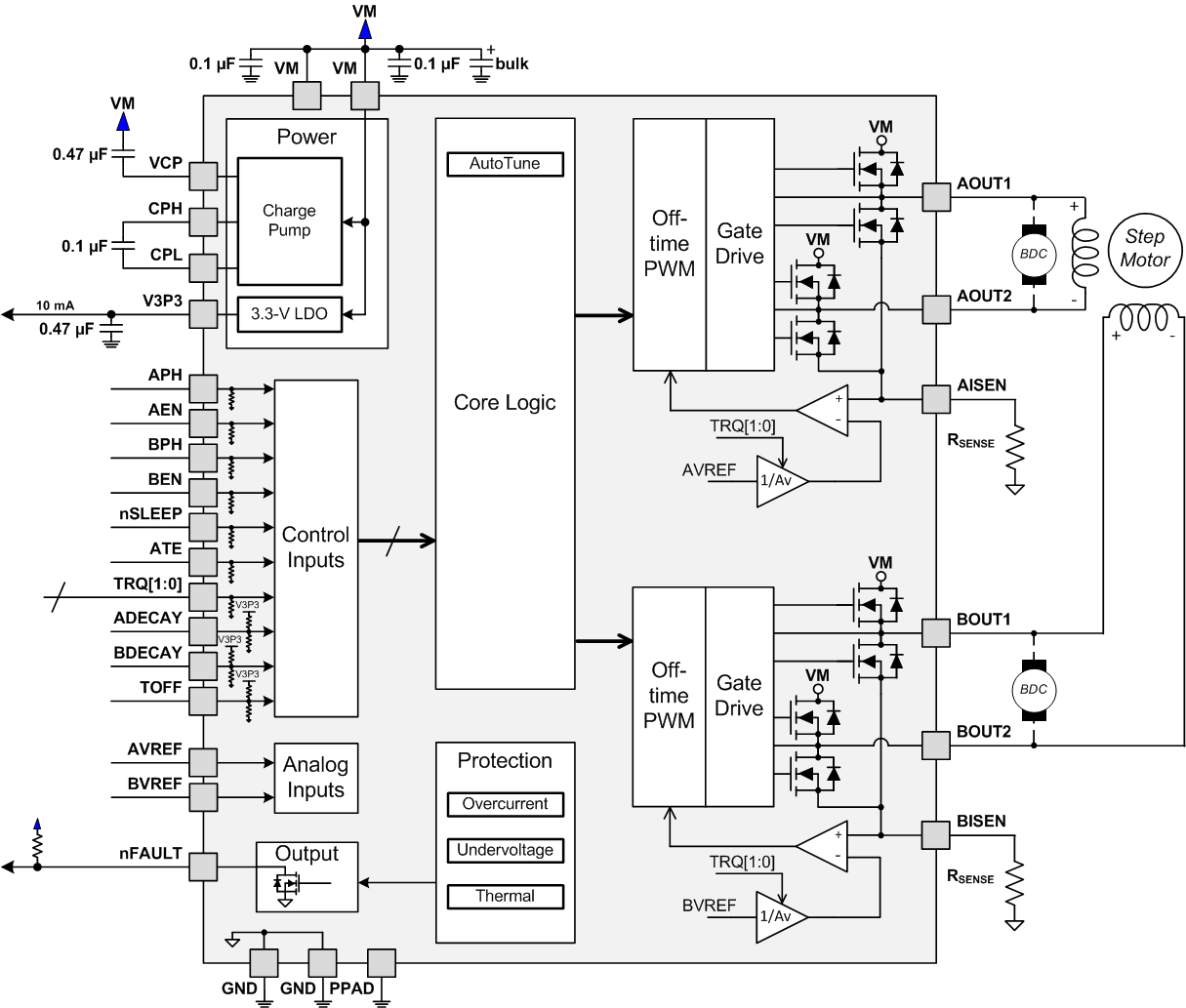 Figure 11. DRV8881E Block Diagram
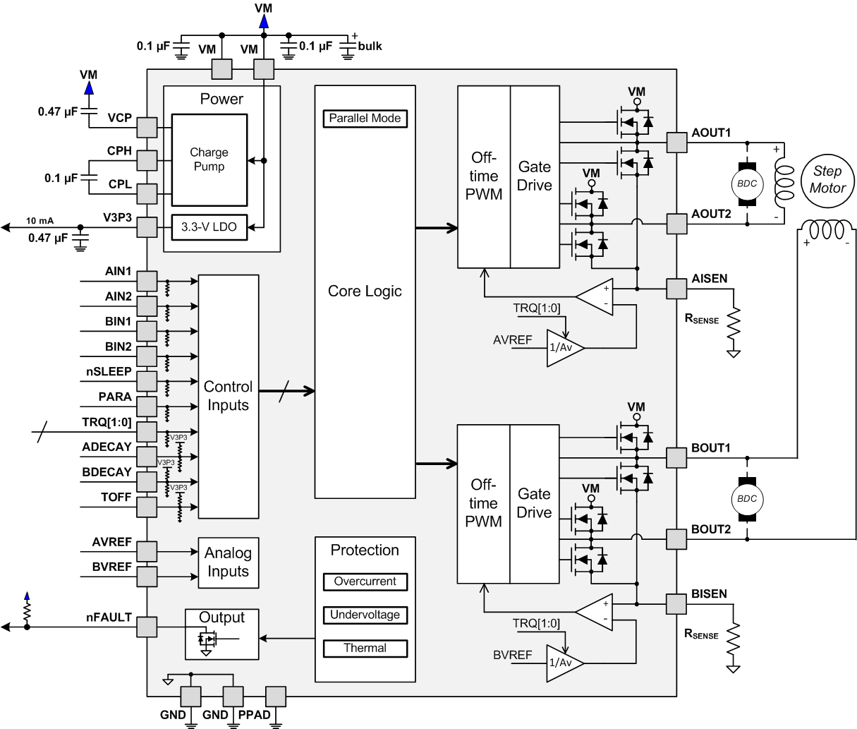 Figure 12. DRV8881P Block Diagram
7.3 Feature Description
7.3.1 Motor Driver Current Ratings
Brushed motor drivers can be classified using two different numbers to describe the output current: peak and rms. Stepper motor drivers can be described with three numbers: peak, rms, and full-scale.
7.3.1.1 Peak Current Rating
The peak current in a motor driver is limited by the overcurrent protection trip threshold IOCP. The peak current describes any transient duration current pulse, for example when charging capacitance, when the overall duty cycle is very low. In general the minimum value of IOCP specifies the peak current rating of the motor driver. For the DRV8881, the peak current rating is 2.5 A per bridge.
7.3.1.2 RMS Current Rating
The rms (average) current is determined by the thermal considerations of the IC. The rms current is calculated based on the RDS(ON), rise and fall time, PWM frequency, device quiescent current, and package thermal performance in a typical system at 25°C. The real operating rms current may be higher or lower depending on heatsinking and ambient temperature. For the DRV8881, the rms current rating is 1.4 A per bridge. In parallel mode, the DRV8881P is capable of double the rms output current, or 2.8 A.
7.3.1.3 Full-Scale Current Rating
The full-scale current for a stepper motor describes the top of the sinusoid current waveform while stepping. Since the sineusoid amplitude is related to the rms current, the full-scale current is also determined by the thermal considerations of the IC. The full-scale current rating is approximately √2 × Irms. The full-scale current is set by xVREF, the sense resistor, and Torque DAC when configuring the DRV8881. For the DRV8881, the full-scale current rating is 2.0 A per bridge.
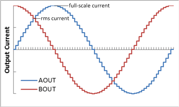 Figure 13. Full-Scale and rms Current
7.3.2 PWM Motor Drivers
The DRV8881 contains drivers for two full H-bridges. Figure 14 shows a block diagram of the circuitry.
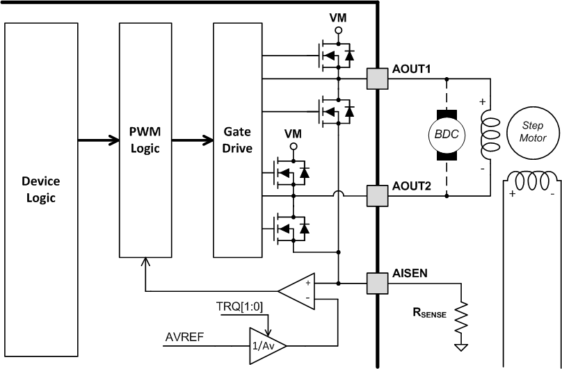 Figure 14. PWM Motor Driver Block Diagram
7.3.3 Bridge Control
The DRV8881E is controlled using a PH/EN interface. Table 1 gives the full H-bridge state. Note that this table does not take into account the current control built into the DRV8881E. Positive current is defined in the direction of xOUT1 → xOUT2.
Table 1. DRV8881E (PH/EN) Control Interface
| nSLEEP | ENx | PHx | xOUT1 | xOUT2 | V3P3 | DESCRIPTION |
|---|---|---|---|---|---|---|
| 0 | X | X | Hi-Z | Hi-Z | Disabled | Sleep mode; H-bridge disabled Hi-Z |
| 1 | 0 | X | Hi-Z | Hi-Z | Enabled | H-bridge disabled Hi-Z |
| 1 | 1 | 0 | L | H | Enabled | Reverse (current xOUT2 → xOUT1) |
| 1 | 1 | 1 | H | L | Enabled | Forward (current xOUT1 → xOUT2) |
The DRV8881P is controlled using a PWM interface. Table 2 gives the full H-bridge state. Note that this table does not take into account the current control built into the DRV8881P. Positive current is defined in the direction of xOUT1 → xOUT2.
Table 2. DRV8881P (PWM) Control Interface
| nSLEEP | xIN1 | xIN2 | xOUT1 | xOUT2 | V3P3 | DESCRIPTION |
|---|---|---|---|---|---|---|
| 0 | X | X | Hi-Z | Hi-Z | Disabled | Sleep mode; H-bridge disabled Hi-Z |
| 1 | 0 | 0 | Hi-Z | Hi-Z | Enabled | Coast; H-bridge disabled Hi-Z |
| 1 | 0 | 1 | L | H | Enabled | Reverse (current xOUT2 → xOUT1) |
| 1 | 1 | 0 | H | L | Enabled | Forward (current xOUT1 → xOUT2) |
| 1 | 1 | 1 | L | L | Enabled | Brake; low-side slow decay |
7.3.4 Current Regulation
The current through the motor windings is regulated by an adjustable fixed-off-time PWM current regulation circuit. When an H-bridge is enabled, current rises through the winding at a rate dependent on the DC voltage, inductance of the winding, and the magnitude of the back EMF present. Once the current hits the current chopping threshold, the bridge enters a decay mode for a fixed period of time to decrease the current, which is configurable between 10 and 30 µs through the tri-level input TOFF. After the off time expires, the bridge is re-enabled, starting another PWM cycle.
Table 3. Off-Time Settings
| TOFF | OFF-TIME tOFF |
|---|---|
| 0 | 20 µs |
| 1 | 30 µs |
| Z | 10 µs |
The PWM chopping current is set by a comparator which compares the voltage across a current sense resistor connected to the xISEN pin with a reference voltage. To generate the reference voltage for the current chopping comparator, the xVREF input is attenuated by a factor of Av. In addition, the TRQx pins further scale the reference.
 Figure 15. Current Regulation Block Diagram
The chopping current is calculated as follows:

TRQ is a DAC used to scale the output current. The current scalar value for different inputs is shown in Table 4.
Table 4. Torque DAC Settings
| TRQ1 | TRQ0 | CURRENT SCALAR (TRQ) | EFFECTIVE ATTENUATION |
|---|---|---|---|
| 1 | 1 | 25% | 26.4 V/V |
| 1 | 0 | 50% | 13.2 V/V |
| 0 | 1 | 75% | 8.8 V/V |
| 0 | 0 | 100% | 6.6 V/V |
7.3.5 Decay Modes
A fixed decay mode is selected by setting the tri-level ADECAY and BDECAY pins as shown in Table 5. Note that if the ATE pin is logic high, the ADECAY and BDECAY pins are ignored and AutoTune is used.
Table 5. Decay Mode Settings
| xDECAY | DECAY MODE |
|---|---|
| 0 | Slow decay |
| Z | Fast decay |
| 1 | Mixed decay: 30% fast |
The ADECAY pin sets the decay mode for H-bridge A (AOUT1, AOUT2), and the BDECAY pin sets the decay mode for H-bridge B (BOUT1, BOUT2).
7.3.5.1 Mode 1: Slow Decay
To configure the DRV8881 into this mode, pull DECAY1 and DECAY0 logic low.
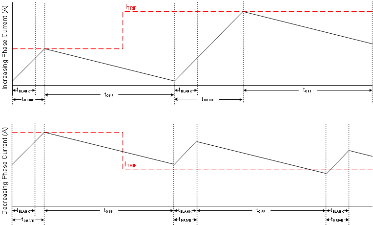 Figure 16. Slow Decay Mode
During slow decay, both of the low-side FETs of the H-bridge are turned on, allowing the current to be recirculated.
Slow decay exhibits the least current ripple of the decay modes for a given tOFF. However, if the current trip level is decreasing, slow decay will take a long time to settle to the new ITRIP level because the current decreases very slowly.
7.3.5.2 Mode 2: Fast Decay
To configure the DRV8881 into this mode, pull DECAY1 and DECAY0 logic high.
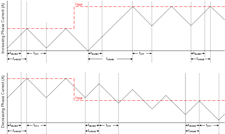 Figure 17. Fast Decay Mode
During fast decay, the polarity of the H-bridge is reversed. The H-bridge will be turned off as current approaches zero in order to prevent current flow in the reverse direction.
Fast decay exhibits the highest current ripple of the decay modes for a given tOFF. Transition time on decreasing current is much faster than slow decay since the current is allowed to decrease much faster.
7.3.5.3 Mode 3: 30%/70% Mixed Decay
To configure the DRV8881 into this mode, pull DECAY1 logic high and pull DECAY0 logic low.
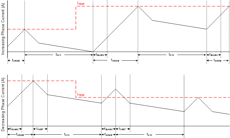 Figure 18. Mixed Decay Mode (30% Fast, 70% Slow)
Mixed decay begins as fast decay for 30% of tOFF, followed by slow decay for the remainder of tOFF. In this mode, mixed decay occurs for both increasing and decreasing current steps.
This mode exhibits ripple larger than slow decay, but smaller than fast decay. Mixed decay will settle to the new ITRIP level faster than slow decay when dealing with decreasing current trip levels.
In cases where current is held for a long time or at very-low stepping speeds, slow decay may not properly regulate current because no back-EMF is present across the motor windings. In this state, motor current can rise very quickly, and requires an excessively large off-time. Increasing/decreasing mixed decay mode allows the current level to stay in regulation when no back-EMF is present across the motor windings.
7.3.6 AutoTune
AutoTune is available on DRV8881E only.
To enable the AutoTune mode, pull the ATE pin logic high. Ensure the xDECAY pins are logic low. The AutoTune mode is registered internally when exiting from sleep mode or the power-up sequence. The ATE pin can be shorted to V3P3 to pull it logic high for this purpose.
AutoTune greatly simplifies the decay mode selection by automatically configuring the decay mode between slow, mixed, and fast decay. In mixed decay, AutoTune dynamically adjusts the fast decay percentage of the total mixed decay time. This feature eliminates motor tuning by automatically determining the best decay setting that results in the lowest ripple for the motor.
The decay mode setting is optimized iteratively each PWM cycle. If the motor current overshoots the target trip level, then the decay mode becomes more aggressive (add fast decay percentage) on the next cycle in order to prevent regulation loss. If there is a long drive time to reach the target trip level, the decay mode becomes less aggressive (remove fast decay percentage) on the next cycle in order to operate with less ripple and more efficiently.
AutoTune will automatically adjust the decay scheme based on operating factors like:
- Motor winding resistance and inductance
- Motor aging effects
- Motor dynamic speed and load
- Motor supply voltage variation
- Motor back-EMF difference on rising and falling steps
- Low-current vs. high-current dI/dt
7.3.7 Adaptive Blanking Time
After the current is enabled in an H-bridge, the voltage on the xISEN pin is ignored for a period of time before enabling the current sense circuitry. Note that the blanking time also sets the minimum drive time of the PWM.
The time tBLANK is determined by VREF and the torque DAC setting. The timing information for tBLANK is given in Table 6.
Table 6. Adaptive Blanking Time Settings over Torque DAC and xVREF Input Voltage
| xVREF | TORQUE DAC TRQ[1:0] SETTING | |||
|---|---|---|---|---|
| 00 - 100% | 01 - 75% | 10 - 50% | 11 - 25% | |
| 2.475 → 3.300 V | 1.80 µs | 1.50 µs | 1.20 µs | 0.90 µs |
| 1.650 → 2.475 V | 1.50 µs | 1.20 µs | 0.90 µs | 0.90 µs |
| 0.825 → 1.650 V | 1.20 µs | 0.90 µs | 0.90 µs | 0.90 µs |
| 0.000 → 0.825 V | 0.90 µs | 0.90 µs | 0.90 µs | 0.90 µs |
7.3.8 Parallel Mode
To enter parallel mode on the DRV8881P, the PARA pin must be logic high during device power-up or when exiting the sleep mode. The PARA pin can be shorted to V3P3 to pull it logic high for this purpose.
In this mode, the AIN1 and AIN2 pins control the state of the outputs and the BIN1 and BIN2 pins are ignored. Similarly, the ADECAY pin controls the decay mode of the output and AVREF is used as the analog reference voltage. The BIN1, BIN2, BDECAY, and BVREF pins can be tied to GND or left Hi-Z.
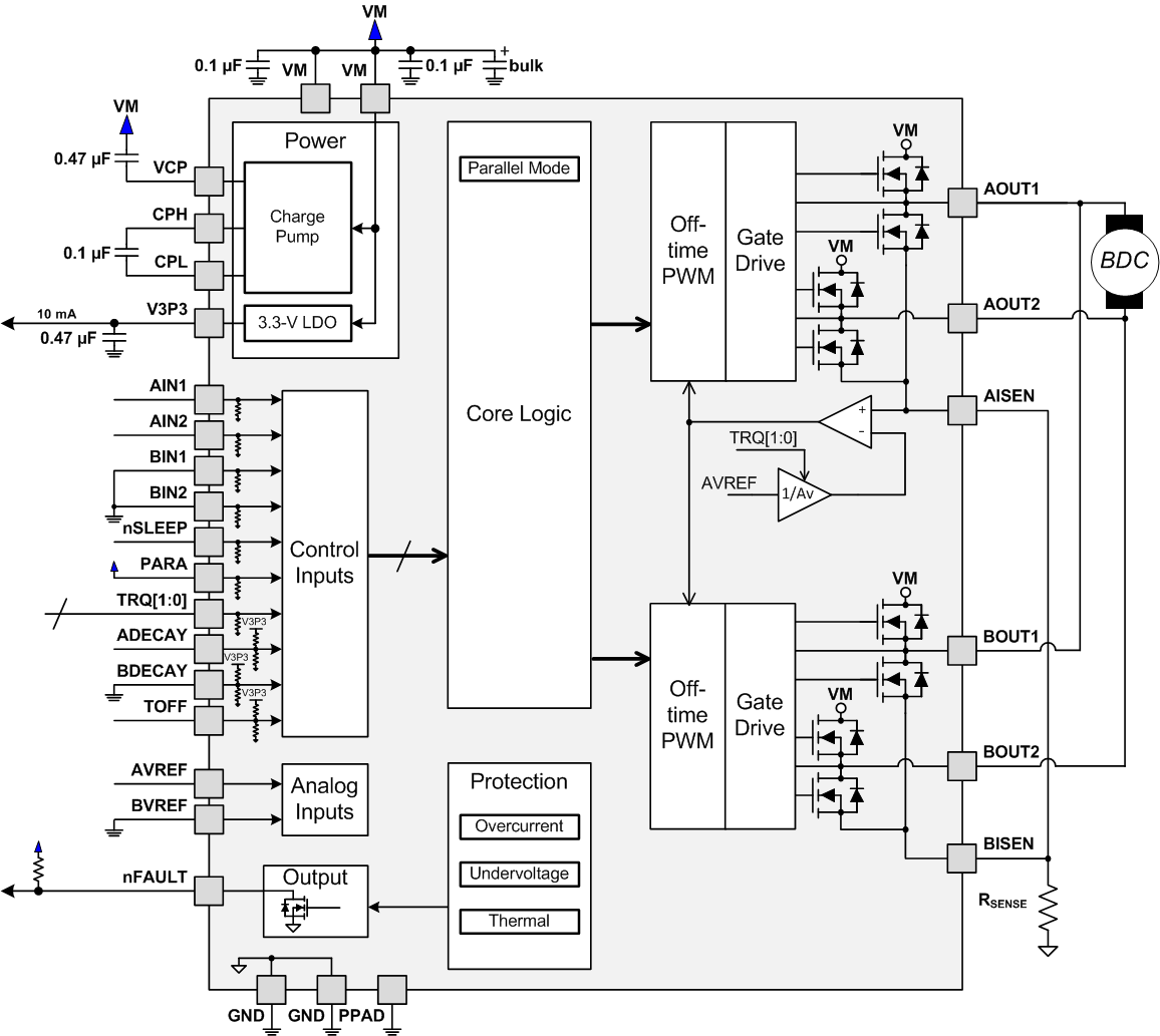 Figure 19. Parallel Mode Diagram
7.3.9 Charge Pump
A charge pump is integrated in order to supply a high-side NMOS gate drive voltage. The charge pump requires a capacitor between the VM and VCP pins. Additionally a low-ESR ceramic capacitor is required between pins CPH and CPL.
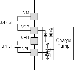 Figure 20. Charge Pump Diagram
7.3.10 LDO Voltage Regulator
An LDO regulator is integrated into the DRV8881. It can be used to provide the supply voltage for a low-power microcontroller or other low-current devices. For proper operation, bypass V3P3 to GND using a ceramic capacitor.
The V3P3 output is nominally 3.3 V. When the V3P3 LDO current load exceeds 10 mA, the LDO will behave like a constant current source. The output voltage will drop significantly with currents greater than 10 mA.
 Figure 21. LDO Diagram
If a digital input needs to be tied permanently high (that is, TOFF or ADECAY), it is preferable to tie the input to V3P3 instead of an external regulator. This will save power when VM is not applied or in sleep mode: V3P3 is disabled and current will not be flowing through the input pulldown resistors. For reference, logic level inputs have a typical pulldown of 100 kΩ, and tri-level inputs have a typical pulldown of 40 kΩ.
7.3.11 Logic and Tri-Level Pin Diagrams
Figure 22 gives the input structure for logic-level pins APH/AIN1, AEN/AIN2, BPH/BIN1, BEN/BIN2, nSLEEP, ATE/PARA, TRQ0, TRQ1:
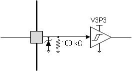 Figure 22. Logic-level Input Pin Diagram
Tri-level logic pins TOFF, ADECAY, and BDECAY have the following structure as shown in Figure 23.
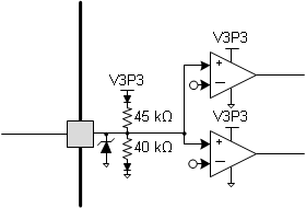 Figure 23. Tri-Level Input Pin Diagram
7.3.12 Protection Circuits
The DRV8881 is fully protected against VM undervoltage, charge pump undervoltage, overcurrent, and overtemperature events.
7.3.12.1 VM Undervoltage Lockout (UVLO)
If at any time the voltage on the VM pin falls below the undervoltage lockout threshold voltage, all FETs in the H-bridge will be disabled, the charge pump will be disabled, and the nFAULT pin will be driven low. Operation will resume when VM rises above the UVLO threshold. The nFAULT pin will be released after operation has resumed.
7.3.12.2 VCP UVLO (CPUV)
If at any time the voltage on the VCP pin falls below the undervoltage lockout threshold voltage, all FETs in the H-bridge will be disabled and the nFAULT pin will be driven low. Operation will resume when VCP rises above the CPUV threshold. The nFAULT pin will be released after operation has resumed.
7.3.12.3 Overcurrent Protection (OCP)
An analog current limit circuit on each FET limits the current through the FET by removing the gate drive. If this analog current limit persists for longer than tOCP, all FETs in the H-bridge will be disabled and nFAULT will be driven low. In addition to this FET current limit, an overcurrent condition is also detected if the voltage at xISEN exceeds VOCP.
For the DRV8881E (PH/EN), both H-bridges are shut down when either bridge encounters an overcurrent fault. For the DRV8881P (PWM), only the H-bridge driver experiencing the overcurrent fault is shut down, and the other bridge will remain active.
The driver will be re-enabled after the OCP retry period (tRETRY) has passed. nFAULT becomes high again after the retry time. If the fault condition is still present, the cycle repeats. If the fault is no longer present, normal operation resumes and nFAULT remains deasserted.
7.3.12.4 Thermal Shutdown (TSD)
If the die temperature exceeds safe limits, all FETs in the H-bridge will be disabled and the nFAULT pin will be driven low. After the die temperature has fallen to a safe level, operation will automatically resume. The nFAULT pin will be released after operation has resumed.
Table 7. Fault Condition Summary
| FAULT | CONDITION | ERROR REPORT | H-BRIDGE | CHARGE PUMP | V3P3 | RECOVERY |
|---|---|---|---|---|---|---|
| VM undervoltage (UVLO) | VM < VUVLO
(max 6.4 V) |
nFAULT | Disabled | Disabled | Operating | VM > VUVLO
(max 6.5 V) |
| VCP undervoltage (CPUV) | VCP < VCPUV
(typ VM + 1.8 V) |
nFAULT | Disabled | Operating | Operating | VCP > VCPUV
(typ VM + 1.9 V) |
| Thermal shutdown (TSD) | TJ > TTSD
(min 150°C) |
nFAULT | Disabled | Operating | Operating | TJ < TTSD- THYS
(THYS typ 35°C) |
| Overcurrent (OCP) | IOUT > IOCP
(min 2.5 A) VxISEN > VOCP (min 0.9 V) |
nFAULT | Disabled | Operating | Operating | tRETRY |
7.4 Device Functional Modes
The DRV8881 is active unless the nSLEEP pin is brought logic low. In sleep mode the charge pump is disabled, the H-bridge FETs are disabled Hi-Z, and the V3P3 regulator is disabled. Note that tSLEEP must elapse after a falling edge on the nSLEEP pin before the device is in sleep mode. The DRV8881 is brought out of sleep mode automatically if nSLEEP is brought logic high. Note that tWAKE must elapse before the outputs change state after wake-up.
Table 8. Functional Modes Summary
| FAULT | CONDITION | H-BRIDGE | CHARGE PUMP | V3P3 |
|---|---|---|---|---|
| Operating | 6.5 V < VM < 45 V nSLEEP pin = 1 |
Operating | Operating | Operating |
| Sleep mode | 6.5 V < VM < 45 V nSLEEP pin = 0 |
Disabled | Disabled | Disabled |
| Fault encountered | VM undervoltage (UVLO) | Disabled | Disabled | Operating |
| VCP undervoltage (CPUV) | Disabled | Operating | Operating | |
| Overcurrent (OCP) | Disabled | Operating | Operating | |
| Thermal shutdown (TSD) | Disabled | Operating | Operating |