ZHCSFZ1A January 2017 – July 2018 DRV8886
UNLESS OTHERWISE NOTED, this document contains PRODUCTION DATA.
- 1 特性
- 2 应用
- 3 说明
- 4 修订历史记录
- 5 Pin Configuration and Functions
- 6 Specifications
-
7 Detailed Description
- 7.1 Overview
- 7.2 Functional Block Diagram
- 7.3
Feature Description
- 7.3.1 Stepper Motor Driver Current Ratings
- 7.3.2 PWM Motor Drivers
- 7.3.3 Microstepping Indexer
- 7.3.4 Current Regulation
- 7.3.5 Controlling RREF With an MCU DAC
- 7.3.6 Decay Modes
- 7.3.7 Blanking Time
- 7.3.8 Charge Pump
- 7.3.9 Linear Voltage Regulators
- 7.3.10 Logic and Multi-Level Pin Diagrams
- 7.3.11 Protection Circuits
- 7.4 Device Functional Modes
- 8 Application and Implementation
- 9 Power Supply Recommendations
- 10Layout
- 11器件和文档支持
- 12机械、封装和可订购信息
封装选项
机械数据 (封装 | 引脚)
散热焊盘机械数据 (封装 | 引脚)
订购信息
7.3.6 Decay Modes
The DRV8886 decay mode is selected by setting the quad-level DECAY pin to the voltage range listed in Table 6. The decay mode setting can be modified during device operation.
Table 6. Decay Mode Settings
| DECAY | INCREASING STEPS | DECREASING STEPS |
|---|---|---|
| 100 mV
Can be tied to ground |
Slow decay | Mixed decay: 30% fast |
| 300 mV, 15 kΩ to GND | Mixed decay: 30% fast | Mixed decay: 30% fast |
| 1 V, 45 kΩ to GND | Mixed decay: 60% fast | Mixed decay: 60% fast |
| 2.9 V
Can be tied to DVDD |
Slow decay | Slow decay |
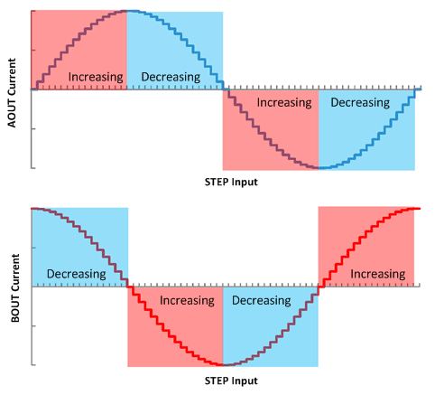
Figure 17 defines increasing and decreasing current. For the slow-mixed decay mode, the decay mode is set as slow during increasing current steps and mixed decay during decreasing current steps. In full step mode the decreasing steps decay mode is always used. In noncircular 1/2-step mode the increasing step decay mode is used after a level transition (0% to 100% and 0% to –100%). When the level transition is to a similar level (100% to 100% and –100% to –100%), the decreasing step decay mode is used.
 Figure 17. Definition of Increasing and Decreasing Steps