ZHCSFZ1A January 2017 – July 2018 DRV8886
UNLESS OTHERWISE NOTED, this document contains PRODUCTION DATA.
- 1 特性
- 2 应用
- 3 说明
- 4 修订历史记录
- 5 Pin Configuration and Functions
- 6 Specifications
-
7 Detailed Description
- 7.1 Overview
- 7.2 Functional Block Diagram
- 7.3
Feature Description
- 7.3.1 Stepper Motor Driver Current Ratings
- 7.3.2 PWM Motor Drivers
- 7.3.3 Microstepping Indexer
- 7.3.4 Current Regulation
- 7.3.5 Controlling RREF With an MCU DAC
- 7.3.6 Decay Modes
- 7.3.7 Blanking Time
- 7.3.8 Charge Pump
- 7.3.9 Linear Voltage Regulators
- 7.3.10 Logic and Multi-Level Pin Diagrams
- 7.3.11 Protection Circuits
- 7.4 Device Functional Modes
- 8 Application and Implementation
- 9 Power Supply Recommendations
- 10Layout
- 11器件和文档支持
- 12机械、封装和可订购信息
封装选项
机械数据 (封装 | 引脚)
散热焊盘机械数据 (封装 | 引脚)
订购信息
7.3.9 Linear Voltage Regulators
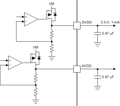
An linear voltage regulator is integrated into the DRV8886 device. The DVDD regulator can be used to provide a reference voltage. For proper operation, bypass the DVDD pin to GND using a ceramic capacitor.
The DVDD output is nominally 3.3 V. When the DVDD LDO current load exceeds 1 mA, the output voltage drops significantly.
The AVDD pin also requires a bypass capacitor to GND. This LDO is for DRV8886 internal use only.
 Figure 22. Linear Voltage Regulator Block Diagram
 If a digital input must be tied permanently high (that is, Mx, DECAY or TRQ), tying the input to the DVDD pin instead of an external regulator is preferred. This method saves power when the VM pin is not applied or in sleep mode: the DVDD regulator is disabled and current does not flow through the input pulldown resistors. For reference, logic level inputs have a typical pulldown of 100 kΩ, and tri-level inputs have a typical pulldown of 60 kΩ.