ZHCSJB5B September 2019 – December 2019 DRV8904-Q1 , DRV8906-Q1 , DRV8908-Q1 , DRV8910-Q1 , DRV8912-Q1
UNLESS OTHERWISE NOTED, this document contains PRODUCTION DATA.
- 1 特性
- 2 应用
- 3 说明
- 4 修订历史记录
- 5 Device Comparison Table
- 6 Pin Configuration and Functions
- 7 Specifications
-
8 Detailed Description
- 8.1 Overview
- 8.2 Functional Block Diagram
- 8.3
Feature Description
- 8.3.1
Half Bridge Drivers
- 8.3.1.1
Control Modes
- 8.3.1.1.1 Continuous Mode (Without PWM)
- 8.3.1.1.2 Chopping Mode (With PWM)
- 8.3.1.1.3 Parallel Mode (Continuous Operation)
- 8.3.1.1.4
Parallel Mode (PWM Operation)
- 8.3.1.1.4.1 PWM Configuration
- 8.3.1.1.4.2 Free-Wheeling Mode (Synchronous Rectification) Disable / Enable
- 8.3.1.1.4.3 PWM Channels Mapping
- 8.3.1.1.4.4 PWM Channels Configuration (PWM Frequency and PWM Duty)
- 8.3.1.1.4.5 PWM Generators Disable
- 8.3.1.1.4.6 Half-Bridge Enable
- 8.3.1.1.4.7 PWM Generators Enable
- 8.3.1.2 Half-Bridge Drive Architecture
- 8.3.1.1
Control Modes
- 8.3.2 Pin Diagrams
- 8.3.3 Protection Circuits
- 8.3.1
Half Bridge Drivers
- 8.4 Device Functional Modes
- 8.5 Programming
- 8.6
Register Map
- 8.6.1
DRV8912-Q1 and DRV8910-Q1 Register Maps
- 8.6.1.1
Status Registers
- 8.6.1.1.1 IC Status (IC_STAT) Register (Address = 0x00) [reset = 0x00]
- 8.6.1.1.2 Overcurrent Protection (OCP) Status 1 (OCP_STAT_1) Register (Address = 0x01) [reset = 0x00]
- 8.6.1.1.3 Overcurrent Protection (OCP) Status 2 (OCP_STAT_2) Register (Address = 0x02) [reset = 0x00]
- 8.6.1.1.4 Overcurrent Protection (OCP) Status 3 (OCP_STAT_3) Register (Address = 0x03) [reset = 0x00]
- 8.6.1.1.5 Open-Load Detect (OLD) Status 1 (OLD_STAT_1) Register (Address = 0x04) [reset = 0x00]
- 8.6.1.1.6 Open-Load Detect (OLD) Status 2 (OLD_STAT_2) Register (Address = 0x05) [reset = 0x00]
- 8.6.1.1.7 Open-Load Detect (OLD) Status 3 (OLD_STAT_3) Register (Address = 0x06) [reset = 0x00]
- 8.6.1.2
Control Registers
- 8.6.1.2.1 Configuration (CONFIG_CTRL) Register (Address = 0x07) [reset = 0x00]
- 8.6.1.2.2 Operation Control 1 (OP_CTRL_1) Register (Address = 0x08) [reset = 0x00]
- 8.6.1.2.3 Operation Control 2 (OP_CTRL_2) Register (Address = 0x09) [reset = 0x00]
- 8.6.1.2.4 Operation Control 3 (OP_CTRL_3) Register (Address = 0x0A) [reset = 0x00]
- 8.6.1.2.5 PWM Control 1 (PWM_CTRL_1) Register (Address = 0x0B) [reset = 0x00]
- 8.6.1.2.6 PWM Control 2 (PWM_CTRL_2) Register (Address = 0x0C) [reset = 0x00]
- 8.6.1.2.7 Free-Wheeling Control 1 (FW_CTRL_1) Register (Address = 0x0D) [reset = 0x00]
- 8.6.1.2.8 Free-Wheeling Control 2 (FW_CTRL_2) Register (Address = 0x0E) [reset = 0x00]
- 8.6.1.2.9 PWM Map Control 1 (PWM_MAP_CTRL_1) Register (Address = 0x0F) [reset = 0x00]
- 8.6.1.2.10 PWM Map Control 2 (PWM_MAP_CTRL_2) Register (Address = 0x10) [reset = 0x00]
- 8.6.1.2.11 PWM Map Control 3 (PWM_MAP_CTRL_3) Register (Address = 0x11) [reset = 0x00]
- 8.6.1.2.12 PWM Frequency Control (PWM_FREQ_CTRL) Register (Address = 0x12) [reset = 0x00]
- 8.6.1.2.13 PWM Duty Control Channel 1 (PWM_DUTY_CH1) Register (Address = 0x13) [reset = 0x00]
- 8.6.1.2.14 PWM Duty Control Channel 2 (PWM_DUTY_CH2) Register (Address = 0x14) [reset = 0x00]
- 8.6.1.2.15 PWM Duty Control Channel 3 (PWM_DUTY_CH3) Register (Address = 0x15) [reset = 0x00]
- 8.6.1.2.16 PWM Duty Control Channel 4 (PWM_DUTY_CH4) Register (Address = 0x16) [reset = 0x00]
- 8.6.1.2.17 Slew Rate Control 1 (SR_CTRL_1) Register (Address = 0x17) [reset = 0x00]
- 8.6.1.2.18 Slew Rate Control 2 (SR_CTRL_2) Register (Address = 0x18) [reset = 0x00]
- 8.6.1.2.19 Open-Load Detect (OLD) Control 1 (OLD_CTRL_1) Register (Address = 0x19) [reset = 0x00]
- 8.6.1.2.20 Open-Load Detect (OLD) Control 2 (OLD_CTRL_2) Register (Address = 0x1A) [reset = 0x00]
- 8.6.1.2.21 Open-Load Detect (OLD) Control 3 (OLD_CTRL_3) Register (Address = 0x1B) [reset = 0x00]
- 8.6.1.2.22 Open-Load Detect (OLD) Control 4 (OLD_CTRL_4) Register (Address = 0x24) [reset = 0x00]
- 8.6.1.1
Status Registers
- 8.6.2
DRV8908-Q1, DRV8906-Q1 and DRV8904-Q1 Register Maps
- 8.6.2.1
Status Registers
- 8.6.2.1.1 IC Status (IC_STAT) Register (Address = 0x00) [reset = 0x00]
- 8.6.2.1.2 Overcurrent Protection (OCP) Status 1 (OCP_STAT_1) Register (Address = 0x01) [reset = 0x00]
- 8.6.2.1.3 Overcurrent Protection (OCP) Status 2 (OCP_STAT_2) Register (Address = 0x02) [reset = 0x00]
- 8.6.2.1.4 Overcurrent Protection (OCP) Status 3 (OCP_STAT_3) Register (Address = 0x03) [reset = 0x00]
- 8.6.2.1.5 Open-Load Detect (OLD) Status 1 (OLD_STAT_1) Register (Address = 0x04) [reset = 0x00]
- 8.6.2.1.6 Open-Load Detect (OLD) Status 2 (OLD_STAT_2) Register (Address = 0x05) [reset = 0x00]
- 8.6.2.1.7 Open-Load Detect (OLD) Status 3 (OLD_STAT_3) Register (Address = 0x06) [reset = 0x00]
- 8.6.2.2
Control Registers
- 8.6.2.2.1 Configuration (CONFIG_CTRL) Register (Address = 0x07) [reset = 0x00]
- 8.6.2.2.2 Operation Control 1 (OP_CTRL_1) Register (Address = 0x08) [reset = 0x00]
- 8.6.2.2.3 Operation Control 2 (OP_CTRL_2) Register (Address = 0x09) [reset = 0x00]
- 8.6.2.2.4 Operation Control 3 (OP_CTRL_3) Register (Address = 0x0A) [reset = 0x00]
- 8.6.2.2.5 PWM Control 1 (PWM_CTRL_1) Register (Address = 0x0B) [reset = 0x00]
- 8.6.2.2.6 PWM Control 2 (PWM_CTRL_2) Register (Address = 0x0C) [reset = 0x00]
- 8.6.2.2.7 Free-Wheeling Control 1 (FW_CTRL_1) Register (Address = 0x0D) [reset = 0x00]
- 8.6.2.2.8 Free-Wheeling Control 2 (FW_CTRL_2) Register (Address = 0x0E) [reset = 0x00]
- 8.6.2.2.9 PWM Map Control 1 (PWM_MAP_CTRL_1) Register (Address = 0x0F) [reset = 0x00]
- 8.6.2.2.10 PWM Map Control 2 (PWM_MAP_CTRL_2) Register (Address = 0x10) [reset = 0x00]
- 8.6.2.2.11 PWM Map Control 3 (PWM_MAP_CTRL_3) Register (Address = 0x11) [reset = 0x00]
- 8.6.2.2.12 PWM Map Control 4 (PWM_MAP_CTRL_4) Register (Address = 0x12) [reset = 0x00]
- 8.6.2.2.13 PWM Frequency Control 1 (PWM_FREQ_CTRL_1) Register (Address = 0x13 [reset = 0x00]
- 8.6.2.2.14 PWM Frequency Control 2 (PWM_FREQ_CTRL_2) Register (Address = 0x14 [reset = 0x00]
- 8.6.2.2.15 PWM Duty Control Channel 1 (PWM_DUTY_CH1) Register (Address = 0x15) [reset = 0x00]
- 8.6.2.2.16 PWM Duty Control Channel 2 (PWM_DUTY_CH2) Register (Address = 0x16) [reset = 0x00]
- 8.6.2.2.17 PWM Duty Control Channel 3 (PWM_DUTY_CH3) Register (Address = 0x17) [reset = 0x00]
- 8.6.2.2.18 PWM Duty Control Channel 4 (PWM_DUTY_CH4) Register (Address = 0x18) [reset = 0x00]
- 8.6.2.2.19 PWM Duty Control Channel 5 (PWM_DUTY_CH5) Register (Address = 0x19) [reset = 0x00]
- 8.6.2.2.20 PWM Duty Control Channel 6 (PWM_DUTY_CH6) Register (Address = 0x1A) [reset = 0x00]
- 8.6.2.2.21 PWM Duty Control Channel 7 (PWM_DUTY_CH7) Register (Address = 0x1B) [reset = 0x00]
- 8.6.2.2.22 PWM Duty Control Channel 8 (PWM_DUTY_CH8) Register (Address = 0x1C) [reset = 0x00]
- 8.6.2.2.23 Slew Rate Control 1 (SR_CTRL_1) Register (Address = 0x1D [reset = 0x00]
- 8.6.2.2.24 Slew Rate Control 2 (SR_CTRL_2) Register (Address = 0x1E) [reset = 0x00]
- 8.6.2.2.25 Open-Load Detect (OLD) Control 1 (OLD_CTRL_1) Register (Address = 0x1F) [reset = 0x00]
- 8.6.2.2.26 Open-Load Detect (OLD) Control 2 (OLD_CTRL_2) Register (Address = 0x20) [reset = 0x00]
- 8.6.2.2.27 Open-Load Detect (OLD) Control 3 (OLD_CTRL_3) Register (Address = 0x21) [reset = 0x00]
- 8.6.2.2.28 Open Load Detect (OLD) Control 4 (OLD_CTRL_4) Register (Address = 0x22) [reset = 0x00]
- 8.6.2.2.29 Open Load Detect (OLD) Control 5 (OLD_CTRL_5) Register (Address = 0x23) [reset = 0x00]
- 8.6.2.2.30 Open Load Detect (OLD) Control 6 (OLD_CTRL_6) Register (Address = 0x24) [reset = 0x00]
- 8.6.2.1
Status Registers
- 8.6.1
DRV8912-Q1 and DRV8910-Q1 Register Maps
- 9 Application and Implementation
- 10Power Supply Recommendations
- 11Layout
- 12器件和文档支持
- 13机械、封装和可订购信息
8.3.1.1.1 Continuous Mode (Without PWM)
The half-bridges are configured to operate in the continuous mode without using any PWM switching by default. Any high-side or low-side switch is switched on by individually setting the high-side enable bits (HBX_HS_EN) and low-side enable bits (HBX_LS_EN) in operation control registers (OP_CTRL_1, OP_CTRL_2 and OP_CTRL_3).
NOTE
If the high-side enable bit (HBX_HS_EN) and low-side enable bit (HBX_LS_EN) of a particular half-bridge is set high (shoot-through configuration), then the particular half-bridge driver will remain in Hi-Z state until he shoot-through condition is cleared.
The high-side and low-side enable bits of a particular half-bridge are configured to drive the motor in forward mode, reverse mode, brake mode and coast mode as shown in Table 2.
Table 2. Motor Operation in Continuous Mode (Motor Connected between HB1 and HB2)
| nSLEEP | HALF-BRIDGE-1 | HALF-BRIDGE-2 | OUT1 | OUT2 | BRIDGE OPERATION
(DC MOTOR) |
|---|---|---|---|---|---|
| 0 | HB1_HS_EN = Don't Care
HB1_LS_EN = Don't Care |
HB2_HS_EN = Don't Care
HB2_LS_EN = Don't Care |
Z | Z | Sleep Mode |
| 1 | HB1_HS_EN = 0
HB1_LS_EN = 0 |
HB2_HS_EN = 0
HB2_LS_EN = 0 |
Z | Z | Motor Coast |
| 1 | HB1_HS_EN = 1
HB1_LS_EN = 0 |
HB2_HS_EN = 0
HB2_LS_EN = 1 |
H | L | Forward Direction |
| 1 | HB1_HS_EN = 0
HB1_LS_EN = 1 |
HB2_HS_EN = 1
HB2_LS_EN = 0 |
L | H | Reverse Direction |
| 1 | HB1_HS_EN = 0
HB1_LS_EN =1 |
HB2_HS_EN = 0
HB2_LS_EN = 1 |
L | L | Motor Brake (Low-Side) |
| 1 | HB1_HS_EN =1
HB1_LS_EN = 0 |
HB2_HS_EN = 1
HB2_LS_EN = 0 |
H | H | Motor Brake (High-Side) |
| 1 | HB1_HS_EN = 1
HB1_LS_EN = 1 |
HB2_HS_EN = 1
HB2_LS_EN = 1 |
Z | Z | Motor Coast |
Figure 24 shows the bridge configuration for motor operation in forward direction with high-side FET of OUT1 and low-side FET of OUT2 in conducting state with current flowing from OUT1 to OUT2. Similarly, the motor operation in reverse direction is achieved by switching ON the high-side FET of OUT2 and low-side FET of OUT1 such that current flows from OUT2 to OUT1 as shown in Figure 25.
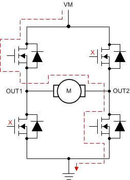 Figure 24. Continuous Mode (Forward Direction)
 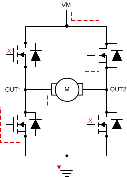 Figure 25. Continuous Mode (Reverse Direction)
 Figure 26 and Figure 27 shows the bridge operation in coast mode with motor initially running in forward and reverse direction respectively. As shown in these figures, due to the energy stored in motor's inductance, the current will continue to flow in motor and take the path flow through the body diodes of FETs.
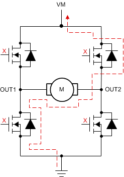 Figure 26. Continuous Mode (Coast - From Forward Direction)
 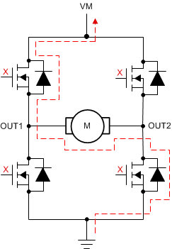 Figure 27. Continuous Mode (Coast- From Reverse Direction)
 Figure 28 shows the low-side braking of the motor when both low-side FET's of the driver are turned ON. In this case, the motor is considered to be operating in forward direction (current flow from OUT1 to OUT2) and then braking is applied. similarly, for the high-side braking, both high-side FET's of the driver are turned ON as shown in Figure 29.
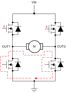 Figure 28. Continuous Mode (Brake - Low-Side)
 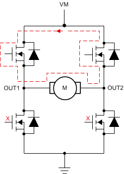 Figure 29. Continuous Mode (Brake - High-Side)