ZHCSJB5B September 2019 – December 2019 DRV8904-Q1 , DRV8906-Q1 , DRV8908-Q1 , DRV8910-Q1 , DRV8912-Q1
UNLESS OTHERWISE NOTED, this document contains PRODUCTION DATA.
- 1 特性
- 2 应用
- 3 说明
- 4 修订历史记录
- 5 Device Comparison Table
- 6 Pin Configuration and Functions
- 7 Specifications
-
8 Detailed Description
- 8.1 Overview
- 8.2 Functional Block Diagram
- 8.3
Feature Description
- 8.3.1
Half Bridge Drivers
- 8.3.1.1
Control Modes
- 8.3.1.1.1 Continuous Mode (Without PWM)
- 8.3.1.1.2 Chopping Mode (With PWM)
- 8.3.1.1.3 Parallel Mode (Continuous Operation)
- 8.3.1.1.4
Parallel Mode (PWM Operation)
- 8.3.1.1.4.1 PWM Configuration
- 8.3.1.1.4.2 Free-Wheeling Mode (Synchronous Rectification) Disable / Enable
- 8.3.1.1.4.3 PWM Channels Mapping
- 8.3.1.1.4.4 PWM Channels Configuration (PWM Frequency and PWM Duty)
- 8.3.1.1.4.5 PWM Generators Disable
- 8.3.1.1.4.6 Half-Bridge Enable
- 8.3.1.1.4.7 PWM Generators Enable
- 8.3.1.2 Half-Bridge Drive Architecture
- 8.3.1.1
Control Modes
- 8.3.2 Pin Diagrams
- 8.3.3 Protection Circuits
- 8.3.1
Half Bridge Drivers
- 8.4 Device Functional Modes
- 8.5 Programming
- 8.6
Register Map
- 8.6.1
DRV8912-Q1 and DRV8910-Q1 Register Maps
- 8.6.1.1
Status Registers
- 8.6.1.1.1 IC Status (IC_STAT) Register (Address = 0x00) [reset = 0x00]
- 8.6.1.1.2 Overcurrent Protection (OCP) Status 1 (OCP_STAT_1) Register (Address = 0x01) [reset = 0x00]
- 8.6.1.1.3 Overcurrent Protection (OCP) Status 2 (OCP_STAT_2) Register (Address = 0x02) [reset = 0x00]
- 8.6.1.1.4 Overcurrent Protection (OCP) Status 3 (OCP_STAT_3) Register (Address = 0x03) [reset = 0x00]
- 8.6.1.1.5 Open-Load Detect (OLD) Status 1 (OLD_STAT_1) Register (Address = 0x04) [reset = 0x00]
- 8.6.1.1.6 Open-Load Detect (OLD) Status 2 (OLD_STAT_2) Register (Address = 0x05) [reset = 0x00]
- 8.6.1.1.7 Open-Load Detect (OLD) Status 3 (OLD_STAT_3) Register (Address = 0x06) [reset = 0x00]
- 8.6.1.2
Control Registers
- 8.6.1.2.1 Configuration (CONFIG_CTRL) Register (Address = 0x07) [reset = 0x00]
- 8.6.1.2.2 Operation Control 1 (OP_CTRL_1) Register (Address = 0x08) [reset = 0x00]
- 8.6.1.2.3 Operation Control 2 (OP_CTRL_2) Register (Address = 0x09) [reset = 0x00]
- 8.6.1.2.4 Operation Control 3 (OP_CTRL_3) Register (Address = 0x0A) [reset = 0x00]
- 8.6.1.2.5 PWM Control 1 (PWM_CTRL_1) Register (Address = 0x0B) [reset = 0x00]
- 8.6.1.2.6 PWM Control 2 (PWM_CTRL_2) Register (Address = 0x0C) [reset = 0x00]
- 8.6.1.2.7 Free-Wheeling Control 1 (FW_CTRL_1) Register (Address = 0x0D) [reset = 0x00]
- 8.6.1.2.8 Free-Wheeling Control 2 (FW_CTRL_2) Register (Address = 0x0E) [reset = 0x00]
- 8.6.1.2.9 PWM Map Control 1 (PWM_MAP_CTRL_1) Register (Address = 0x0F) [reset = 0x00]
- 8.6.1.2.10 PWM Map Control 2 (PWM_MAP_CTRL_2) Register (Address = 0x10) [reset = 0x00]
- 8.6.1.2.11 PWM Map Control 3 (PWM_MAP_CTRL_3) Register (Address = 0x11) [reset = 0x00]
- 8.6.1.2.12 PWM Frequency Control (PWM_FREQ_CTRL) Register (Address = 0x12) [reset = 0x00]
- 8.6.1.2.13 PWM Duty Control Channel 1 (PWM_DUTY_CH1) Register (Address = 0x13) [reset = 0x00]
- 8.6.1.2.14 PWM Duty Control Channel 2 (PWM_DUTY_CH2) Register (Address = 0x14) [reset = 0x00]
- 8.6.1.2.15 PWM Duty Control Channel 3 (PWM_DUTY_CH3) Register (Address = 0x15) [reset = 0x00]
- 8.6.1.2.16 PWM Duty Control Channel 4 (PWM_DUTY_CH4) Register (Address = 0x16) [reset = 0x00]
- 8.6.1.2.17 Slew Rate Control 1 (SR_CTRL_1) Register (Address = 0x17) [reset = 0x00]
- 8.6.1.2.18 Slew Rate Control 2 (SR_CTRL_2) Register (Address = 0x18) [reset = 0x00]
- 8.6.1.2.19 Open-Load Detect (OLD) Control 1 (OLD_CTRL_1) Register (Address = 0x19) [reset = 0x00]
- 8.6.1.2.20 Open-Load Detect (OLD) Control 2 (OLD_CTRL_2) Register (Address = 0x1A) [reset = 0x00]
- 8.6.1.2.21 Open-Load Detect (OLD) Control 3 (OLD_CTRL_3) Register (Address = 0x1B) [reset = 0x00]
- 8.6.1.2.22 Open-Load Detect (OLD) Control 4 (OLD_CTRL_4) Register (Address = 0x24) [reset = 0x00]
- 8.6.1.1
Status Registers
- 8.6.2
DRV8908-Q1, DRV8906-Q1 and DRV8904-Q1 Register Maps
- 8.6.2.1
Status Registers
- 8.6.2.1.1 IC Status (IC_STAT) Register (Address = 0x00) [reset = 0x00]
- 8.6.2.1.2 Overcurrent Protection (OCP) Status 1 (OCP_STAT_1) Register (Address = 0x01) [reset = 0x00]
- 8.6.2.1.3 Overcurrent Protection (OCP) Status 2 (OCP_STAT_2) Register (Address = 0x02) [reset = 0x00]
- 8.6.2.1.4 Overcurrent Protection (OCP) Status 3 (OCP_STAT_3) Register (Address = 0x03) [reset = 0x00]
- 8.6.2.1.5 Open-Load Detect (OLD) Status 1 (OLD_STAT_1) Register (Address = 0x04) [reset = 0x00]
- 8.6.2.1.6 Open-Load Detect (OLD) Status 2 (OLD_STAT_2) Register (Address = 0x05) [reset = 0x00]
- 8.6.2.1.7 Open-Load Detect (OLD) Status 3 (OLD_STAT_3) Register (Address = 0x06) [reset = 0x00]
- 8.6.2.2
Control Registers
- 8.6.2.2.1 Configuration (CONFIG_CTRL) Register (Address = 0x07) [reset = 0x00]
- 8.6.2.2.2 Operation Control 1 (OP_CTRL_1) Register (Address = 0x08) [reset = 0x00]
- 8.6.2.2.3 Operation Control 2 (OP_CTRL_2) Register (Address = 0x09) [reset = 0x00]
- 8.6.2.2.4 Operation Control 3 (OP_CTRL_3) Register (Address = 0x0A) [reset = 0x00]
- 8.6.2.2.5 PWM Control 1 (PWM_CTRL_1) Register (Address = 0x0B) [reset = 0x00]
- 8.6.2.2.6 PWM Control 2 (PWM_CTRL_2) Register (Address = 0x0C) [reset = 0x00]
- 8.6.2.2.7 Free-Wheeling Control 1 (FW_CTRL_1) Register (Address = 0x0D) [reset = 0x00]
- 8.6.2.2.8 Free-Wheeling Control 2 (FW_CTRL_2) Register (Address = 0x0E) [reset = 0x00]
- 8.6.2.2.9 PWM Map Control 1 (PWM_MAP_CTRL_1) Register (Address = 0x0F) [reset = 0x00]
- 8.6.2.2.10 PWM Map Control 2 (PWM_MAP_CTRL_2) Register (Address = 0x10) [reset = 0x00]
- 8.6.2.2.11 PWM Map Control 3 (PWM_MAP_CTRL_3) Register (Address = 0x11) [reset = 0x00]
- 8.6.2.2.12 PWM Map Control 4 (PWM_MAP_CTRL_4) Register (Address = 0x12) [reset = 0x00]
- 8.6.2.2.13 PWM Frequency Control 1 (PWM_FREQ_CTRL_1) Register (Address = 0x13 [reset = 0x00]
- 8.6.2.2.14 PWM Frequency Control 2 (PWM_FREQ_CTRL_2) Register (Address = 0x14 [reset = 0x00]
- 8.6.2.2.15 PWM Duty Control Channel 1 (PWM_DUTY_CH1) Register (Address = 0x15) [reset = 0x00]
- 8.6.2.2.16 PWM Duty Control Channel 2 (PWM_DUTY_CH2) Register (Address = 0x16) [reset = 0x00]
- 8.6.2.2.17 PWM Duty Control Channel 3 (PWM_DUTY_CH3) Register (Address = 0x17) [reset = 0x00]
- 8.6.2.2.18 PWM Duty Control Channel 4 (PWM_DUTY_CH4) Register (Address = 0x18) [reset = 0x00]
- 8.6.2.2.19 PWM Duty Control Channel 5 (PWM_DUTY_CH5) Register (Address = 0x19) [reset = 0x00]
- 8.6.2.2.20 PWM Duty Control Channel 6 (PWM_DUTY_CH6) Register (Address = 0x1A) [reset = 0x00]
- 8.6.2.2.21 PWM Duty Control Channel 7 (PWM_DUTY_CH7) Register (Address = 0x1B) [reset = 0x00]
- 8.6.2.2.22 PWM Duty Control Channel 8 (PWM_DUTY_CH8) Register (Address = 0x1C) [reset = 0x00]
- 8.6.2.2.23 Slew Rate Control 1 (SR_CTRL_1) Register (Address = 0x1D [reset = 0x00]
- 8.6.2.2.24 Slew Rate Control 2 (SR_CTRL_2) Register (Address = 0x1E) [reset = 0x00]
- 8.6.2.2.25 Open-Load Detect (OLD) Control 1 (OLD_CTRL_1) Register (Address = 0x1F) [reset = 0x00]
- 8.6.2.2.26 Open-Load Detect (OLD) Control 2 (OLD_CTRL_2) Register (Address = 0x20) [reset = 0x00]
- 8.6.2.2.27 Open-Load Detect (OLD) Control 3 (OLD_CTRL_3) Register (Address = 0x21) [reset = 0x00]
- 8.6.2.2.28 Open Load Detect (OLD) Control 4 (OLD_CTRL_4) Register (Address = 0x22) [reset = 0x00]
- 8.6.2.2.29 Open Load Detect (OLD) Control 5 (OLD_CTRL_5) Register (Address = 0x23) [reset = 0x00]
- 8.6.2.2.30 Open Load Detect (OLD) Control 6 (OLD_CTRL_6) Register (Address = 0x24) [reset = 0x00]
- 8.6.2.1
Status Registers
- 8.6.1
DRV8912-Q1 and DRV8910-Q1 Register Maps
- 9 Application and Implementation
- 10Power Supply Recommendations
- 11Layout
- 12器件和文档支持
- 13机械、封装和可订购信息
8.3.3.5.1.1 Negative-current OLD
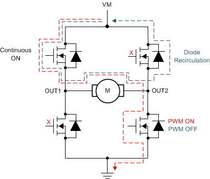
The DRV89XX-Q1 device also includes a negative-current OLD mode. The negative current can flow either through the body diode of high-side FET or the FET itself depending on whether or not the channel is configured for synchronous rectification. Figure 54 shows the current re-circulation through the body diode of the high-side FET when the synchronous rectification mode is OFF (i.e. HB2_FW = 0). In this case, the active OLD will not falsely report an open-load condition since the OLD circuit only enables when the FET is ON. Negative-current OLD will also work during re-circulation through the low-side FETs.
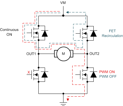
Figure 55 shows the negative current re-circulation through the high-side FET when synchronous rectification is ON (i.e. HB2_FW = 1). In this scenario, for default operation (OLD_NEG_EN = 0), the device can show a false open-load fault since the FET current is lower than the positive OLD threshold. However, when negative-current OLD mode is enabled, the device will only flag an open-load fault if IOUTX < IOLD_NEG. This mode is enabled by setting the OLD_NEG_EN bit in OLD_CTRL3 register.
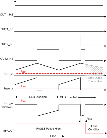
Figure 56 shows the waveforms of false open-load detection when the negative-current OLD setting is disabled (OLD_NEG_EN = 0). As shown in this figure, the high-side FET of the OUT1 channel is always switched ON and the low-side and high-side FET of the OUT2 channel are operating in complimentary way (i.e. synchronous rectification mode is enabled). In synchronous rectification, the current flows in negative direction from OUT2 to VM (i.e. FET Source to Drain) during the high-side FET conduction. Initially, for the first PWM cycle, the OLD mode is disabled to show the currents in different FETs during the motor operation. When OLD is enabled in second PWM cycle, then the device registers a false open-load detect during the high-side FET conduction as shown in Figure 56. The nFAULT pin is pulled low and both high-side and low-side FET of OUT2 channels are disabled. The body diode of the high side FET (OUT2) conducts to complete the motor current path.
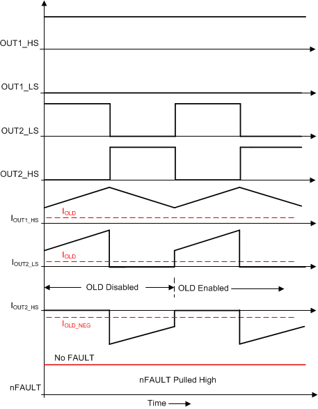
This false detection of open load is eliminated by enabling the negative-current OLD setting (OLD_NEG_EN = 1). As shown in Figure 57, the negative OLD current setting (IOLD_NEG) is enabled for the high-side FET of OUT2 channel. This setting allows the negative current path (from source to drain) in high-side FET. The nFAULT pin is latched high and OUT2 channel is not disabled when OLD is enabled in second PWM cycle.
 Figure 54. Negative Current Flow in OUT2 by Body Diode of High-Side FET
  Figure 55. Negative Current Flow in High-Side FET of OUT2 Channel
  Figure 56. Waveforms Showing False OLD With Negative-Current OLD Disabled
  Figure 57. Waveforms Showing Operation with Negative-Current OLD Enabled