ZHCS749B January 2012 – January 2015 DS100DF410
PRODUCTION DATA.
- 1 特性
- 2 应用
- 3 说明
- 4 修订历史记录
- 5 Pin Configuration and Functions
- 6 Specifications
-
7 Detailed Description
- 7.1 Overview
- 7.2 Functional Block Diagram
- 7.3
Feature Description
- 7.3.1 Device Data Path Operation
- 7.3.2 Signal Detect
- 7.3.3 CTLE
- 7.3.4 DFE
- 7.3.5 Clock and Data Recovery
- 7.3.6 Output Driver
- 7.3.7 CTLE Boost Setting
- 7.3.8 DFE Tap Weight and Polarity Setting
- 7.3.9 Driver Output Voltage
- 7.3.10 Driver Output De-Emphasis
- 7.3.11 Driver Output Rise/Fall Time
- 7.3.12 Ref_mode 0 Mode (Reference Clock Not Required)
- 7.3.13 Ref_mode 3 Mode (Reference Clock Required)
- 7.3.14 False Lock Detector Setting
- 7.3.15 Reference Clock In
- 7.3.16 Reference Clock Out
- 7.3.17 Daisy Chain of REFCLK_OUT to REFCLK_IN
- 7.3.18 INT
- 7.3.19 LOCK_3, LOCK_2, LOCK_1, and LOCK_0
- 7.4 Device Functional Modes
- 7.5
Programming
- 7.5.1 SMBus Strap Observation
- 7.5.2 Device Revision and Device ID
- 7.5.3 Control/Shared Register Reset
- 7.5.4 Interrupt Channel Flag Bits
- 7.5.5 SMBus Master Mode Control Bits
- 7.5.6 Resetting Individual Channels of the Retimer
- 7.5.7 Interrupt Status
- 7.5.8 Overriding the CTLE Boost Setting
- 7.5.9 Overriding the VCO CAP DAC Values
- 7.5.10 Overriding the Output Multiplexer
- 7.5.11 Overriding the VCO Divider Selection
- 7.5.12 Using the PRBS Generator
- 7.5.13 Using the Internal Eye Opening Monitor
- 7.5.14 Overriding the DFE Tap Weights and Polarities
- 7.5.15 Enabling Slow Rise/Fall Time on the Output Driver
- 7.5.16 Inverting the Output Polarity
- 7.5.17 Overriding the Figure of Merit for Adaptation
- 7.5.18 Setting the Rate and Subrate for Lock Acquisition
- 7.5.19 Setting the Adaptation/Lock Mode
- 7.5.20 Initiating Adaptation
- 7.5.21 Setting the Reference Enable Mode
- 7.5.22 Overriding the CTLE Settings Used for CTLE Adaptation
- 7.5.23 Setting the Output Differential Voltage
- 7.5.24 Setting the Output De-emphasis Setting
- 7.6 Register Maps
- 8 Application and Implementation
- 9 Power Supply Recommendations
- 10Layout
- 11器件和文档支持
- 12机械封装和可订购信息
9 Power Supply Recommendations
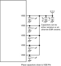
Figure 9 depicts an example power connections diagram for the DS100DF410. The supply (VDD) and ground (GND) Pins should be connected to power planes routed on adjacent layers of the printed circuit board. The layer thickness of the dielectric should be minimized so that the VDD and GND planes create a low inductance supply with distributed capacitance. Second, careful attention to supply bypassing through the proper use of bypass capacitors is required. A 0.1-μF bypass capacitor should be connected to each VDD Pin such that the capacitor is placed as close as possible to the DS100DF410. Smaller body size capacitors can help facilitate proper component placement. Additionally, capacitor with capacitance in the range of 1 μF to 10 μF should be incorporated in the power supply bypassing design as well. These capacitors can be either tantalum or an ultra-low ESR ceramic.
 Figure 9. Example Power Connection