ZHCSDW7A May 2013 – June 2015 DS110DF111
PRODUCTION DATA.
- 1 特性
- 2 应用
- 3 说明
- 4 修订历史记录
- 5 Pin Configuration and Functions
- 6 Specifications
-
7 Detailed Description
- 7.1 Overview
- 7.2 Functional Block Diagram
- 7.3 Feature Description
- 7.4 Device Functional Modes
- 7.5
Programming
- 7.5.1
SMBus Interface
- 7.5.1.1 Address Lines
- 7.5.1.2 Device Configuration in SMBus Slave Mode
- 7.5.1.3 Bit Fields in the Register Set
- 7.5.1.4 Writing to and Reading From the Control/Shared Registers
- 7.5.1.5 SMBus Strap Observation
- 7.5.1.6 Interrupt Channel Flag Bits
- 7.5.1.7 Control/Shared Register Reset
- 7.5.1.8 Device Revision and Device ID
- 7.5.1.9 Channel Select Register
- 7.5.1.10 Resetting Individual Channels of the Retimer
- 7.5.1.11 Rate and Subrate Setting
- 7.5.1.12 Overriding the CTLE Boost Setting
- 7.5.1.13 Overriding the Output Multiplexer
- 7.5.1.14 Overriding the VCO Divider Selection
- 7.5.1.15 Using the Internal Eye Opening Monitor
- 7.5.1.16 Overriding the DFE Tap Weights and Polarities
- 7.5.1.17 Enabling Slow Rise/Fall Time on the Output Driver
- 7.5.1.18 Using the PRBS Generator
- 7.5.1.19 Inverting the Output Polarity
- 7.5.1.20 Overriding the Figure of Merit Adaption
- 7.5.1.21 Setting the Rate and Subrate for Lock Acquisition
- 7.5.1.22 Setting the Adaption/Lock Mode
- 7.5.1.23 Initiating Adaption
- 7.5.1.24 Overriding the CTLE Settings used for CTLE Adaption
- 7.5.1.25 Setting the Output Differential Voltage
- 7.5.1.26 Setting the Output De-Emphasis Setting
- 7.5.1.27 CTLE Setting for Divide by 4 and Divide by 8 VCO Ranges
- 7.5.1
SMBus Interface
- 7.6 Register Maps
- 8 Applications and Implementation
- 9 Power Supply Recommendations
- 10Layout
- 11器件和文档支持
- 12机械、封装和可订购信息
6 Specifications
6.1 Absolute Maximum Ratings(1)
| MIN | MAX | UNIT | |||
|---|---|---|---|---|---|
| Supply Voltage (VDD) | –0.5 | +2.75 | V | ||
| Supply Voltage (VIN) | –0.5 | +4.0 | V | ||
| LVCMOS Input/Output Voltage | –0.5 | +4.0 | V | ||
| 4-Level Input Voltage (2.5 V mode) | –0.5 | +2.75 | V | ||
| 4-Level Input Voltage (3.3 V mode) | –0.5 | 4.0 | V | ||
| SMBus Input/Output Voltage | –0.5 | 4.0 | V | ||
| CML Input Voltage | –0.5 | VDD + 0.5 | V | ||
| CML Input Current | –30 | +30 | mA | ||
| Storage Temperature Tstg | –40 | +125 | °C | ||
(1) For soldering specifications, see product folder at www.ti.com
6.2 ESD Ratings
| VALUE | UNIT | ||
|---|---|---|---|
| ESD Rating(1) | HBM, STD - JESD22-A114F(2) | ±2500 | V |
| CDM, STD - JESD22-C101-D(3) | ±1000 | V | |
(1) Electrostatic discharge (ESD) to measure device sensitivity and immunity to damage caused by assembly line electrostatic discharges in to the device.
(2) Level listed above is the passing level per ANSI, ESDA, and JEDEC JS-001. JEDEC document JEP155 states that 500-V HBM allows safe manufacturing with a standard ESD control process.
(3) Level listed above is the passing level per EIA-JEDEC JESD22-C101. JEDEC document JEP157 states that 250-V CDM allows safe manufacturing with a standard ESD control process.
6.3 Recommended Operating Conditions
| MIN | NOM | MAX | UNIT | ||
|---|---|---|---|---|---|
| Supply Voltage | 2.5 V Mode | 2.375 | 2.5 | 2.625 | V |
| 3.3 V Mode | 3.0 | 3.3 | 3.6 | ||
| Ambient Temperature | –40 | 25 | +85 | °C | |
| SMBus (SDA, SCL) | 3.0 | 3.3 | 3.6 | V | |
6.4 Thermal Information
| THERMAL METRIC(1) | DS110DF111 | UNIT | |
|---|---|---|---|
| WQFN (RTW) | |||
| 24 PINS | |||
| θJA | Junction-to-ambient thermal resistance | 35.0 | °C/W |
| RθJC(top) | Junction-to-case (top) thermal resistance | 34.0 | °C/W |
| RθJB | Junction-to-board thermal resistance | 13.4 | °C/W |
| ψJT | Junction-to-top characterization parameter | 0.3 | °C/W |
| ψJB | Junction-to-board characterization parameter | 13.4 | °C/W |
| RθJC(bot) | Junction-to-case (bottom) thermal resistance | 3.3 | °C/W |
(1) For more information about traditional and new thermal metrics, see the Semiconductor and IC Package Thermal Metrics application report, SPRA953.
6.5 Electrical Characteristics
| PARAMETER | TEST CONDITIONS | MIN | TYP | MAX | UNIT | |
|---|---|---|---|---|---|---|
| R_baud | Input baud rate | Full Rate: DS110DF111 | 8.5 | 11.3 | Gbps | |
| FSDC | SMBus Clock Rate | Slave Mode Clock Rate | 100 | 400 | kHz | |
| Master Mode Clock Rate | 280 | 400 | 520 | |||
| REFCLK | Clock Rate | ± 100 ppm | 25.0 | MHz | ||
| POWER SUPPLY CURRENT | ||||||
| IDD | Current Consumption (Whole Device) |
11.3 Gbps : DS110DF111 | 170 | mA | ||
| 11.3 Gbps : DS110DF111 DFE Disabled |
150 | mA | ||||
| Maximum Transient Supply Current Default Settings: CHA and CHB valid input signal detected CHA and CHB acquiring LOCK |
235 | 300 | mA | |||
| NTps | Supply Noise Tolerance | 50 Hz to 100 Hz | 100 | mVp-p | ||
| 100 Hz to 10 MHz | 40 | mVp-p | ||||
| 10 MHz to 5.0 GHz | 10 | mVp-p | ||||
| LVCMOS (LBK, READEN#, DONE#, LOCK) | ||||||
| VIH | High level input voltage | 2.5 V or 3.3 V Supply Modes | 1.7 | VIN | V | |
| VIL | Low level input voltage | 2.5 V or 3.3 V Supply Modes | 0.7 | |||
| VOH | High level output voltage | IOH = –3 mA | 2.0 | VIN | V | |
| VOL | Low level output voltage | IOL = 3 mA | 0.4 | |||
| IIN | Input leakage current | VINPUT = GND or VIN | –15 | +15 | μA | |
| 4-LEVEL INPUTS (ENSMB, DEMA, DEMB, TX_DIS, VODA, VODB) | ||||||
| IIN-R | Input leakage current | VINPUT = GND or VIN | –160 | +80 | μA | |
| OPEN DRAIN (LOS/INT#) | ||||||
| VOL | Low level output voltage | IOL = 3 mA | 0.4 | V | ||
| SIGNAL DETECT | ||||||
| SDH | Signal Detect: ON Threshold Level |
Default level to assert Signal Detect, 10.3125 Gbps |
20 | mVp-p | ||
| SDL | Signal Detect: OFF Threshold Level |
Default level to de-assert Signal Detect, 10.3125 Gbps |
15 | mVp-p | ||
| CML RX INPUTS | ||||||
| R_Rd | DC Input differential Resistance | 100 | Ω | |||
| RLRX-IN | Input Return-Loss | SDD11 10 MHz | –19 | dB | ||
| SDD11 2.0 GHz | –14 | |||||
| SDD11 6.0 - 11.1 GHz | –8 | |||||
| VRX-LAUNCH | Source Transmit Signal Level | 600 | 1600 | mVp-p | ||
| CML TX OUTPUTS | ||||||
| T_VDIFF0 | Output differential voltage | Default setting, PRBS31 | 400 | 550 | 675 | mVp-p |
| T_VDIFF7 | Output differential voltage | Maximum setting, PRBS31 Requires SMBus Control |
1000 | 1250 | mVp-p | |
| VOD_DE | De-emphasis Level | Maximum setting, VOD and DE Requires SMBus Control Input: 10.3125Gbps, 64T pattern |
–12 | dB | ||
| T_Rd | DC Output Differential Resistance | 100 | Ω | |||
| TR/TF | Output Rise/Fall Time | Full Slew Rate 20% - 80% Input: 10.3125 Gbps, 8T Pattern |
36 | ps | ||
| TRS/TFS | Output Rise/Fall Time | Limited Slew Rate (Reg 0x18) 20% - 80% Input: 10.3125 Gbps, 8T Pattern |
50 | ps | ||
| TSDD22 | Output differential mode return loss | SDD22 10 MHz - 2 GHz | –19 | dB | ||
| SDD22 5.5GHz | –15 | |||||
| SDD22 11.1GHz | –11 | |||||
| TPD | Propagation Delay | Retimed Data 10.3125 Gbps | 350 | ps | ||
| TPD-RAW | Propagation Delay | Raw Data | 200 | ps | ||
| TRANSMIT JITTER SPECS(1) | ||||||
| TTJ | Total Jitter (1E-12) | PRBS7, 10.3125 Gbps | 7.5 | ps | ||
| TRJ | Random Jitter | PRBS7, 10.3125 Gbps | 0.33 | ps (RMS) | ||
| TDJ | Deterministic Jitter | PRBS7, 10.3125 Gbps | 3.6 | ps | ||
| CLOCK AND DATA RECOVERY | ||||||
| BWPLL | PLL Bandwidth –3 dB | Measured at 10.3125 Gbps | 5 | MHz | ||
| JTOL | Total jitter tolerance | Jitter per SFF-8431 Appendix D.11 Combination of Dj, Pj, and Rj |
> 0.70 | UI | ||
| TLOCK1 | CDR Lock Time | Standards Based(2) | 10 - 30 | ms | ||
| TEMPLOCK | CDR Lock | Lock Temperature Range –40°C to 85°C operating range |
125 | °C | ||
| SERIAL BUS INTERFACE CHARACTERISTICS(3) | ||||||
| VIL | Data, Clock Input Low Voltage (SDA / SCL) |
0.8 | V | |||
| VIH | Data, Clock Input High Voltage (SDA / SCL) |
2.1 | 3.6 | V | ||
| VHY | Input Hystersis | >50 | mV | |||
| VOL | Output Low Voltage | SDA or SCL, IOL = 1.25 mA | 0 | 0.36 | V | |
| IIN | Input Current | SDA or SCL, VINPUT = VIN, VDD, GND | –15 | +15 | μA | |
| TR | SDA Rise Time, Read Operation | SDA, RPU = 10K, Cb < 400 pF | 430 | ns | ||
| TF | SDA Fall Time, Read Operation | SDA, RPU = 10K, Cb < 400 pF | 20 | ns | ||
| TSU;DAT | Setup Time, Read Operation | 560 | ns | |||
| THD;DAT | Hold Time, Read Operation | 615 | ns | |||
| TSP | Input Filter | 50 | ns | |||
| CIN | Input Capacitance | SDA or SCL | < 5 | pF | ||
| RECOMMENDED TIMING FOR THE SERIAL BUS INTERFACE | ||||||
| FSCL | SCL Clock Frequency | 400 | kHz | |||
| TLOW | SCL Low Period | 1300 | ns | |||
| THIGH | SCL High Period | 600 | ns | |||
| THD;STA | Hold Time, Start Operation | 600 | ns | |||
| TSU;STA | Setup Time, Start Operation | 600 | ns | |||
| THD;DAT | Data Hold Time | 0 | 900 | ns | ||
| TSU;DAT | Data Set Up Time | 100 | ns | |||
| TSU;STO | Set Up Time, Stop Condition | 600 | ns | |||
| TBUF | Bus Free Time Between Stop - Start |
1300 | ns | |||
| TF | SCL and SDA, Fall Time | 300 | ns | |||
| TR | SCL and SDA, Rise Time | 1000 | ns | |||
(1) Rj and Dj Jitter decomposition as reported by TEK DSA8200 Sampling scope using a 80E09 Electrical sampling module, 80A06 Pattern trigger, and 82A04 Phase Reference Module.
(2) The typical LOCK time can vary based on data-rate, input channel, and specific DS110DF111 settings.
(3) EEPROM interface requires 520 kHz capable (1 MHz Recommended) EEPROM device.
 Figure 1. Output Edge Rate
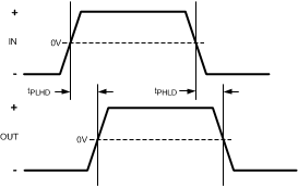
 Figure 2. Propagation Delay
 Figure 3. SMBus Timing Diagram
6.6 Typical Characteristics

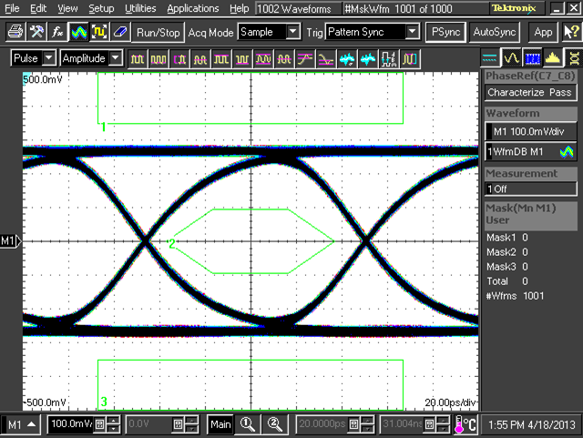
| Test Conditions | ||
| Datarate: 10.3125 Gbps with a PRBS7 pattern | ||
| VOD Setting: 1000mV | ||
| Temperature: 25°C and VDD = 2.5V |

| Jitter Measurements | ||
| Rj (RMS): 315 fs | Dj: 3.74 ps | Tj (1E-12): 7.33 ps |