SNLS472A January 2014 – June 2017 DS110DF1610
PRODUCTION DATA.
- 1Features
- 2Description
- 3Revision History
- 4Pin Configuration and Functions
- 5Specifications
-
6Detailed Description
- 6.1 Overview
- 6.2 Functional Block Diagrams
- 6.3 Feature Description
- 6.4 Device Functional Modes
- 6.5 Programming
- 6.6 Register Maps
- 7Application and Implementation
- 8Power Supply Recommendations
7 Application and Implementation
NOTE
Information in the following applications sections is not part of the TI component specification, and TI does not warrant its accuracy or completeness. TI’s customers are responsible for determining suitability of components for their purposes. Customers should validate and test their design implementation to confirm system functionality.
7.1 Typical Applications
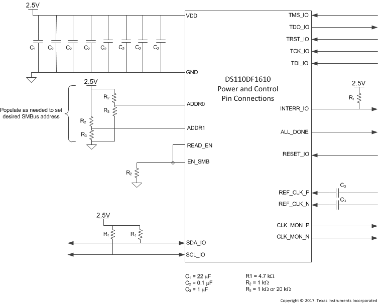
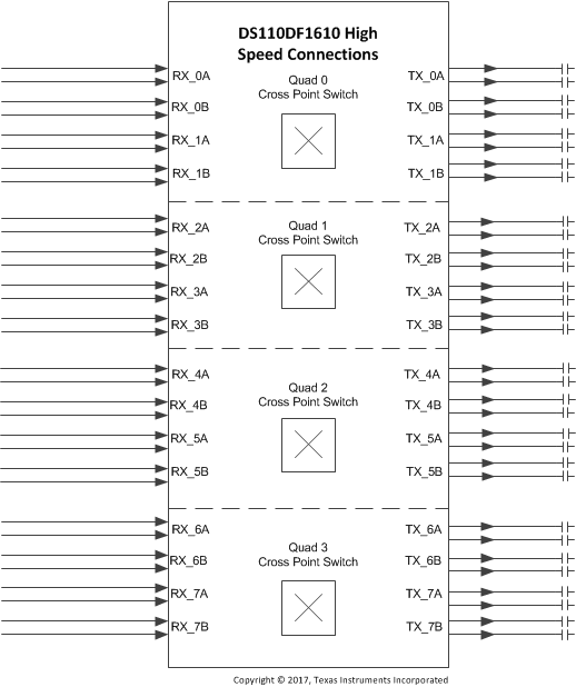
Figure 5 and Figure 6 show a typical application of the DS110Df1610. In these diagrams, the DS110DF1610 is configured for SMBus slave mode programming. Power is supplied to the device through a single 2.5V plane. The power supply filtering shown in these diagrams may need to be adjusted to accommodate additional system power noise. The SMBus and LVCMOS signals in this example use 2.5V logic. A differential reference clock for the digital block is applied to the device through 1µF AC-coupling capacitors. In this example, the high speed signals are connected to the device in groups of four to allow for the system designer to make use of the 4x4 cross point switches. Note that since the device contains AC-coupling capacitors on the high speed receiver inputs, the signals can be directly connected to the device. The transmitter outputs of this device should connect to AC-coupling capacitors placed near the receive inputs of the receiving ASIC.
 Figure 5. Typical Connection Diagram: Power and Control Pins
 Figure 6. Typical Connection Diagram: High Speed Signals
7.2 Initialization Setup
The typical device initialization sequence for a DS110DF1610 includes the following:
- Shared Register Configurations
- Reference Clock Divider Setting (default is 125MHz)
- Lock Sequencer Configuration (default is 8 channels allowed lock concurrently)
- Channel Register Configurations repeated for all desired channels:
- CDR reset
- Adapt Mode Configuration
- Data rate selection
- Output driver VOD and FIR configuration
- Optional Continuous DFE adaption configuration
- Optional Interrupt enable
- Optional Reference clock loop through enable
- Optional Cross point switch configuration
- CDR reset release
7.2.1 Data Rate Selection (Rate/Sub-Rate Table)
The data rates for the DS110DF1610 must be known and programmed into each desired channel. The DS110DF1610 will only lock to programmed data rates and the programmed divider settings. For ease of use several common data rates have been preprogrammed into the DS110DF1610 along with the associated sub-rates for those various standards. These rate/sub-rate settings comprise the Rate/Sub-rate Table. Note that each channel operates independently, so different channels in the DS110DF1610 can operate at different data rates at the same time.
The Rate/Sub-rate table for the DS110DF1610 shown below includes all of the available preprogrammed data rates and associated divider groupings.
| CHANNEL REGISTER 0x2F[7:4] SETTING | STANDARD | DATA RATES (Gbps) | FIRST GROUP DIVIDER SETTINGS | SECOND GROUP DIVIDER SETTINGS |
|---|---|---|---|---|
| 0x0 | Custom 1 | 5.0, 2.5 | 2, 4 | 2, 4 |
| 0xC | Ethernet | 1.25, 10.3125 | 8 | 1 |
| 0xD | Fiber Channel | (2.125, 4.25, 8.5), 10.51875 | 1, 2, 4 | 1 |
| 0xE | SFF 8431 | 9.95328 | 1 | 1 |
| 0xF | Custom 2 | 8.625, 4.3125 | 1, 2 | 1, 2 |
7.2.2 Data Rate Selection (Manual Programming)
The DS110DF1610 is capable of supporting any data rate within the specified range of 8.5 Gbps to 11.3 Gbps including the divide by 2, 4, and 8 sub-rates of this range. If it is desired to operate the DS110DF1610 at a data rate or data rate and sub-rate combination that is not available in the Rate/Sub-rate Table, then these desired data rates can be programmed into the device manually.
The following procedure describes how to calculate and manually program data rates into the DS110DF1610.
- Select a divider grouping from the Rate/Sub-rate Table and program that value to channel register 0x2F. When manually programming the data rate into the device, other rate/sub-rate values may be used to allow for different divider and group combinations. A list of all preprogrammed divider, group combinations is shown in the table below.
- Calculate the first group settings:
- Calculate the second group settings:
| CHANNEL REGISTER 0x2F[7:4] SETTING |
FIRST GROUP DIVIDER SETTINGS | SECOND GROUP DIVIDER SETTINGS |
|---|---|---|
| 0x0 | 2, 4 | 2, 4 |
| 0x1 | 1 | 1 |
| 0x2 | 1, 2, 4 | 1, 2, 4 |
| 0x3 | 1, 2, 4 | 1, 2, 4 |
| 0x4 | 1 | 1 |
| 0x5 | 1 | 1 |
| 0x6 | 1 | 1 |
| 0x7 | 1, 2, 4 | 1, 2, 4 |
| 0x8 | 1, 2, 4 | 1, 2, 4 |
| 0x9 | 2, 4 | 2, 4 |
| 0xA | 1, 2, 4 | 1, 2, 4 |
| 0xB | 8 | 1 |
| 0xC | 8 | 1 |
| 0xD | 1, 2, 4 | 1 |
| 0xE | 1 | 1 |
| 0xF | 1, 2 | 1, 2 |
| PARAMETER | VALUE/EQUATION | COMMENT |
|---|---|---|
| Reference Clock | F0 = 25e6 | Internally the reference clock always operates at 25 MHz |
| Desired VCO Frequency | F1 | F1 is the frequency of the VC0 which is equal to the desired data rate. If the desired data rate uses dividers, be sure to multiply the data rate by the divide setting to get the correct VCO frequency |
| Number of Reference Clocks | N = 1024 | |
| VCO Freq ÷ 32 | F2 = F1 ÷ 32 | |
| Counts of VCO Freq ÷ 32 required | F3 = F2 x N ÷ F0 | |
| Counts of VCO Freq ÷ 32 required rounded | F4 | Round F3 to the nearest integer value. Convert this value to binary. Program the upper 8 bits to ch register 0x61 and the lower 8 bits to ch register 0x60. Be sure to set channel register 0x61[7] to 1 to enable the override function for manual programming. |
| PPM error due to rounding | Err = 1e6 x (F4 – F3) ÷ F3 | |
| Required PPM tolerance | T | Enter the desired PPM tolerance |
| VCO Freq ÷ 32 +PPM tolerance | F5 = (1+ T÷1e6) ÷ F2 | |
| Rounded Counts of the VCO Freq ÷ 32 +PPM tolerance required | F6 = F5 x N ÷ F0 | Round F6 to the nearest integer value |
| PPM Counts delta | F7 = F6 – F3 | Convert this value to binary. Program the most significant bit channel register 0x67[7] and the rest of the bits to channel register 0x64[7:4] |
| PARAMETER | VALUE/EQUATION | COMMENT |
|---|---|---|
| Reference Clock | F0 = 25e6 | Internally the reference clock always operates at 25 MHz |
| Desired VCO Frequency | F1 | F1 is the frequency of the VC0 which is equal to the desired data rate. If the desired data rate uses dividers, be sure to multiply the data rate by the divide setting to get the correct VCO frequency |
| Number of Reference Clocks | N = 1024 | |
| VCO Freq ÷ 32 | F2 = F1 ÷ 32 | |
| Counts of VCO Freq ÷ 32 required | F3 = F2 x N ÷ F0 | |
| Counts of VCO Freq ÷ 32 required rounded | F4 | Round F3 to the nearest integer value. Convert this value to binary. Program the upper 8 bits to ch register 0x63 and the lower 8 bits to ch register 0x62. Be sure to set channel register 0x63[7] to 1 to enable the override function for manual programming. |
| PPM error due to rounding | Err = 1e6 x (F4 – F3) ÷ F3 | |
| Required PPM tolerance | T | Enter the desired PPM tolerance |
| VCO Freq ÷ 32 +PPM tolerance | F5 = (1+ T÷1e6) ÷ F2 | |
| Rounded Counts of the VCO Freq ÷ 32 +PPM tolerance required | F6 = F5 x N ÷ F0 | Round F6 to the nearest integer value |
| PPM Counts delta | F7 = F6 – F3 | Convert this value to binary. Program the most significant bit channel register 0x67[6] and the rest of the bits to channel register 0x64[3:0] |
An example for setting group 0 and group 1 to 11.3 Gbps is shown in the table below.
| CHANNEL REGISTER (HEX) | VALUE |
|---|---|
| 0x60 | 0x80 |
| 0x61 | 0xB8 |
| 0x62 | 0x80 |
| 0x63 | 0xB8 |
| 0x64 | 0xEE |
| 0x67[7:6] | 2'b00 |