ZHCSCD5B April 2014 – January 2017 DS125DF1610
PRODUCTION DATA.
- 1 特性
- 2 应用
- 3 说明
- 4 修订历史记录
- 5 Pin Configuration and Functions
- 6 Specifications
-
7 Detailed Description
- 7.1 Overview
- 7.2 Functional Block Diagram
- 7.3
Feature Description
- 7.3.1 Device Data Path Operation
- 7.3.2 AC-Coupled Receiver with Signal Detect
- 7.3.3 CTLE
- 7.3.4 Cross Point Switch
- 7.3.5 DFE with VGA
- 7.3.6 Clock and Data Recovery
- 7.3.7 Reference Clock
- 7.3.8 Differential Driver with FIR Filter
- 7.3.9 Setting the Output VOD
- 7.3.10 Output Driver Polarity Inversion
- 7.3.11 Driver Output Rise/Fall Time
- 7.3.12 Debug Features
- 7.3.13 Interrupt Signals
- 7.3.14 Other Features
- 7.4 Device Functional Modes
- 7.5 Programming
- 8 Application and Implementation
- 9 Power Supply Recommendations
- 10Layout
- 11器件和文档支持
- 12机械、封装和可订购信息
10 Layout
10.1 Layout Guidelines
The high speed inputs and outputs have been optimized to work with interconnects using a controlled differential impedance of 100Ω. Vias should be used sparingly and must be placed symmetrically for each side of a given differential pair. Whenever differential vias are used the layout must also provide for a low inductance path for the return currents as well. Route the differential signals away from other signals and noise sources on the printed circuit board.
10.2 Layout Example
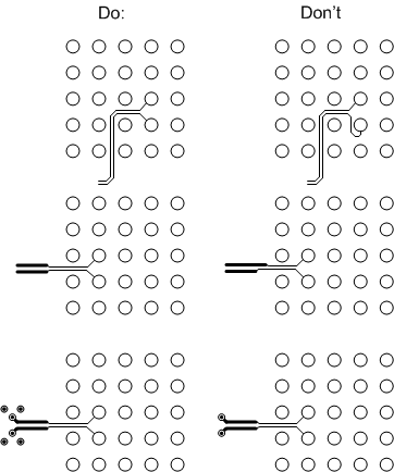
Common BGA routing techniques such as trace necking, using blind vias and buried vias, are OK as long as the differential traces are balanced in their routing and the signals see few impedance changes. For example, necking lengths should be the same for the differential traces and implemented symmetrically for both traces. Figure 10 shows general Dos and Don'ts for high speed layout, such as differential trace gathering, differential trace necking, and high speed signal and return via implementation.
 Figure 10. Layout Guidelines