ZHCSCD5B April 2014 – January 2017 DS125DF1610
PRODUCTION DATA.
- 1 特性
- 2 应用
- 3 说明
- 4 修订历史记录
- 5 Pin Configuration and Functions
- 6 Specifications
-
7 Detailed Description
- 7.1 Overview
- 7.2 Functional Block Diagram
- 7.3
Feature Description
- 7.3.1 Device Data Path Operation
- 7.3.2 AC-Coupled Receiver with Signal Detect
- 7.3.3 CTLE
- 7.3.4 Cross Point Switch
- 7.3.5 DFE with VGA
- 7.3.6 Clock and Data Recovery
- 7.3.7 Reference Clock
- 7.3.8 Differential Driver with FIR Filter
- 7.3.9 Setting the Output VOD
- 7.3.10 Output Driver Polarity Inversion
- 7.3.11 Driver Output Rise/Fall Time
- 7.3.12 Debug Features
- 7.3.13 Interrupt Signals
- 7.3.14 Other Features
- 7.4 Device Functional Modes
- 7.5 Programming
- 8 Application and Implementation
- 9 Power Supply Recommendations
- 10Layout
- 11器件和文档支持
- 12机械、封装和可订购信息
5 Pin Configuration and Functions
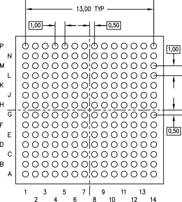
Plastic Ball Grid Array
196 Balls
Bottom View


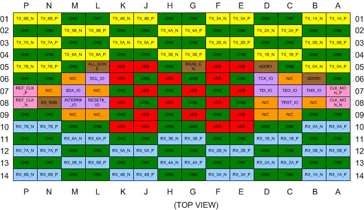
Pin Functions
| DS110DF1610, DS125DF1610 PIN NAME |
DS150DF1610 PIN NAME |
PIN | I/O | DESCRIPTION |
|---|---|---|---|---|
| HIGH SPEED DIFFERENTIAL I/O | ||||
| RX_1A_P RX_1A_N |
RX_0_0P RX_0_0N |
A14 B14 |
I, CML | Inverting and non-inverting CML-compatible, AC coupled differential inputs. An on-chip 100 Ohm differential termination resistor connects these inputs. |
| RX_0B_P Rx_0B_N |
RX_0_1P RX_0_1N |
A12 B12 |
I, CML | Inverting and non-inverting CML-compatible, AC coupled differential inputs. An on-chip 100 Ohm differential termination resistor connects these inputs. |
| RX_0A_P RX_0A_N |
RX_0_2P RX_0_2N |
A10 B10 |
I, CML | Inverting and non-inverting CML-compatible, AC coupled differential inputs. An on-chip 100 Ohm differential termination resistor connects these inputs. |
| RX_2A_P RX_2A_N |
RX_0_3P RX_0_3N |
C13 D13 |
I, CML | Inverting and non-inverting CML-compatible, AC coupled differential inputs. An on-chip 100 Ohm differential termination resistor connects these inputs. |
| RX_1B_P RX_1B_N |
RX_0_4P RX_0_4N |
C11 D11 |
I, CML | Inverting and non-inverting CML-compatible, AC coupled differential inputs. An on-chip 100 Ohm differential termination resistor connects these inputs. |
| RX_3A_P RX_3A_N |
RX_0_5P RX_0_5N |
E14 F14 |
I, CML | Inverting and non-inverting CML-compatible, AC coupled differential inputs. An on-chip 100 Ohm differential termination resistor connects these inputs. |
| RX_2B_P RX_2B_N |
RX_0_6P RX_0_6N |
E12 F12 |
I, CML | Inverting and non-inverting CML-compatible, AC coupled differential inputs. An on-chip 100 Ohm differential termination resistor connects these inputs. |
| RX_4A_P RX_4A_N |
RX_0_7P RX_0_7N |
G13 H13 |
I, CML | Inverting and non-inverting CML-compatible, AC coupled differential inputs. An on-chip 100 Ohm differential termination resistor connects these inputs. |
| RX_3B_P RX_3B_N |
RX_1_0P RX_1_0N |
G11 H11 |
I, CML | Inverting and non-inverting CML-compatible, AC coupled differential inputs. An on-chip 100 Ohm differential termination resistor connects these inputs. |
| RX_4B_P Rx_4B_N |
RX_1_1P RX_1_1N |
J14 K14 |
I, CML | Inverting and non-inverting CML-compatible, AC coupled differential inputs. An on-chip 100 Ohm differential termination resistor connects these inputs. |
| RX_5A_P RX_5A_N |
RX_1_2P RX_1_2N |
J12 K12 |
I, CML | Inverting and non-inverting CML-compatible, AC coupled differential inputs. An on-chip 100 Ohm differential termination resistor connects these inputs. |
| RX_5B_P RX_5B_N |
RX_1_3P RX_1_3N |
L13 M13 |
I, CML | Inverting and non-inverting CML-compatible, AC coupled differential inputs. An on-chip 100 Ohm differential termination resistor connects these inputs. |
| RX_6A_P RX_6A_N |
RX_1_4P RX_1_4N |
L11 M11 |
I, CML | Inverting and non-inverting CML-compatible, AC coupled differential inputs. An on-chip 100 Ohm differential termination resistor connects these inputs. |
| RX_6B_P RX_6B_N |
RX_1_5P RX_1_5N |
N14 P14 |
I, CML | Inverting and non-inverting CML-compatible, AC coupled differential inputs. An on-chip 100 Ohm differential termination resistor connects these inputs. |
| RX_7A_P RX_7A_N |
RX_1_6P RX_1_6N |
N12 P12 |
I, CML | Inverting and non-inverting CML-compatible, AC coupled differential inputs. An on-chip 100 Ohm differential termination resistor connects these inputs. |
| RX_7B_P RX_7B_N |
RX_1_7P RX_1_7N |
N10 P10 |
I, CML | Inverting and non-inverting CML-compatible, AC coupled differential inputs. An on-chip 100 Ohm differential termination resistor connects these inputs. |
| TX_1A_P TX_1A_N |
TX_0_0P TX_0_0N |
A1 B1 |
O, CML | Inverting and non-inverting CML-compatible differential outputs. Driver presents an output impedance of 100 ohms between these outputs when switching. |
| TX_0B_P TX_0B_N |
TX_0_1P TX_0_1N |
A3 B3 |
O, CML | Inverting and non-inverting CML-compatible differential outputs. Driver presents an output impedance of 100 ohms between these outputs when switching. |
| TX_0A_P TX_0A_N |
TX_0_2P TX_0_2N |
A5 B5 |
O, CML | Inverting and non-inverting CML-compatible differential outputs. Driver presents an output impedance of 100 ohms between these outputs when switching. |
| TX_2A_P TX_2A_N |
TX_0_3P TX_0_3N |
C2 D2 |
O, CML | Inverting and non-inverting CML-compatible differential outputs. Driver presents an output impedance of 100 ohms between these outputs when switching. |
| TX_1B_P TX_1B_N |
TX_0_4P TX_0_4N |
C4 D4 |
O, CML | Inverting and non-inverting CML-compatible differential outputs. Driver presents an output impedance of 100 ohms between these outputs when switching. |
| TX_3A_P TX_3A_N |
TX_0_5P TX_0_5N |
E1 F1 |
O, CML | Inverting and non-inverting CML-compatible differential outputs. Driver presents an output impedance of 100 ohms between these outputs when switching. |
| TX_2B_P TX_2B_N |
TX_0_6P TX_0_6N |
E3 F3 |
O, CML | Inverting and non-inverting CML-compatible differential outputs. Driver presents an output impedance of 100 ohms between these outputs when switching. |
| TX_4A_P TX_4A_N |
TX_0_7P TX_0_7N |
G2 H2 |
O, CML | Inverting and non-inverting CML-compatible differential outputs. Driver presents an output impedance of 100 ohms between these outputs when switching. |
| TX_3B_P TX_3B_N |
TX_1_0P TX_1_0N |
G4 H4 |
O, CML | Inverting and non-inverting CML-compatible differential outputs. Driver presents an output impedance of 100 ohms between these outputs when switching. |
| TX_4B_P TX_4B_N |
TX_1_1P TX_1_1N |
J1 K1 |
O, CML | Inverting and non-inverting CML-compatible differential outputs. Driver presents an output impedance of 100 ohms between these outputs when switching. |
| TX_5A_P TX_5A_N |
TX_1_2P TX_1_2N |
J3 K3 |
O, CML | Inverting and non-inverting CML-compatible differential outputs. Driver presents an output impedance of 100 ohms between these outputs when switching. |
| TX_5B_P TX_5B_N |
TX_1_3P TX_1_3N |
L2 M2 |
O, CML | Inverting and non-inverting CML-compatible differential outputs. Driver presents an output impedance of 100 ohms between these outputs when switching. |
| TX_6A_P TX_6A_N |
TX_1_4P TX_1_4N |
L4 M4 |
O, CML | Inverting and non-inverting CML-compatible differential outputs. Driver presents an output impedance of 100 ohms between these outputs when switching. |
| TX_6B_P TX_6B_N |
TX_1_5P TX_1_5N |
N1 P1 |
O, CML | Inverting and non-inverting CML-compatible differential outputs. Driver presents an output impedance of 100 ohms between these outputs when switching. |
| TX_7A_P TX_7A_N |
TX_1_6P TX_1_6N |
N3 P3 |
O, CML | Inverting and non-inverting CML-compatible differential outputs. Driver presents an output impedance of 100 ohms between these outputs when switching. |
| TX_7B_P TX_7B_N |
TX_1_7P TX_1_7N |
N5 P5 |
O, CML | Inverting and non-inverting CML-compatible differential outputs. Driver presents an output impedance of 100 ohms between these outputs when switching. |
| CLOCK PINS | ||||
| REF_CLK_P REF_CLK_N |
P7 P8 |
I, LVDS/ LVCMOS |
Inverting and non-inverting CML-compatible differential inputs for 25 MHz, 125 MHz, or 312.5 MHz clock. These differential signals are typically AC coupled with 1 µF capacitors When configured for single-ended input operation, apply LVCMOS ref clock to REF_CLK_P and float REF_CLK_N. Single-ended signals should be DC coupled. |
|
| CLK_MON_P CLK_MON_N |
A7 A8 |
O, LVDS | Inverting and non-inverting CML-compatible differential outputs to monitor system differential clock. When daisy chaining to another retimer the output frequency should be set to 25 MHz. |
|
| SMBUS INTERFACE | ||||
| SDA_IO | M7 | I/O, Open Drain |
Data Input / Open Drain Output External pull-up resistor is required, typically in the 2kΩ to 5kΩ range. Pull-up value should be selected according to system implementation. Pin is 3.3 V LVCMOS tolerant. |
|
| SCL_IO | L6 | I/O, Open Drain |
Clock input/output External pull-up resistor is required, typically in the 2kΩ to 5kΩ range. Pull-up value should be selected according to system implementation. Pin is 3.3 V LVCMOS tolerant EEPROM configuration (SMBus Master mode) |
|
| JTAG INTERFACE(1) | ||||
| TMS_IO | B7 | I, LVCMOS | JTAG Test Mode Select, internal pull-up | |
| TDO_IO | C7 | O, LVCMOS | JTAG Test Data Out | |
| TRST_IO | C8 | I, LVCMOS | JTAG Test Reset, internal pull-up | |
| TCK_IO | D6 | I, LVCMOS | JTAG Test clock, internal pull-up | |
| TDI_IO | D7 | I, LVCMOS | JTAG Test Data Input, internal pull-up | |
| OTHER PINS | ||||
| RESET_IO | L8 | I, LVCMOS | Resets registers and state machines on rising edge. Pulse LOW for minimum of 10µs to perform reset. Pin should be pulled HIGH during power on. | |
| INTERR_IO | M8 | O, Open Drain | Active Low interrupt signal. Pin goes low when an interrupt event occurs. Interrupts must be enabled via SMBus. | |
| ADDR0 | B6 | I, LVCMOS | 4 level input strap pin for SMBus address code LSB. Standard LVCMOS output. | |
| ADDR1 | D5 | I, LVCMOS | 4 level input strap pin for SMBus address code MSB. Standard LVCMOS output. | |
| READ_EN | G5 | I, LVCMOS | Tie LOW for SMBus slave mode normal operation. Pin has internal pull down. In SMBus slave mode, tie HIGH to force SMBus address = 0x30. |
|
| ALL_DONE | L5 | O, LVCMOS | EEPROM load status. Pin goes LOW when EEPROM load is complete. | |
| EN_SMB | N8 | I, LVCMOS | Connect to GND through ≤1kΩ resistor for SMBus slave operation. Connect to VDD through ≤1kΩ resistor for EEPROM configuration |
|
| POWER | ||||
| VDD | E5, E7, E9, E10, F5, F6, F8, F10, G7, G9, H6, H8, J5, J7, J9, J10, K5, K6, K8, K10 | Power | VDD = 2.5 V +/- 5% | |
| GND | A2, A4, A6, A9, A11, A13, B2, B4, B9, B11, B13, C1, C3, C5, C10, C12, C14, D1, D3, D10, D12, D14, E2, E4, E6, E8, E11, E13, F2, F4, F7, F9, F11, F13, G1, G3, G6, G8, G10, G12, G14, H1, H3, H5, H7, H9, H10, H12, H14, J2, J4, J6, J8, J11, J13, K2, K4, K7, K9, K11, K13, L1, L3, L10, L12, L14, M1, M3, M5, M10, M12, M14, N2, N4, N6, N9, N11, N13, P2, P4, P6, P9, P11, P13 | Power | Ground reference | |
| N/C | B8, C6, C9, D8, D9, L7, L9, M6, M9, N7 | No Connect, leave floating | ||
(1) Refer to the DS125DF1610 Programming Guide for additional information