ZHCSMH6 February 2021 DS160PR421
PRODUCTION DATA
- 1 特性
- 2 应用
- 3 说明
- 4 Revision History
- 5 Pin Configuration and Functions
- 6 Specifications
- 7 Detailed Description
- 8 Application and Implementation
- 9 Power Supply Recommendations
- 10Layout
- 11Layout Example
- 12Device and Documentation Support
- 13Mechanical, Packaging, and Orderable Information
11 Layout Example
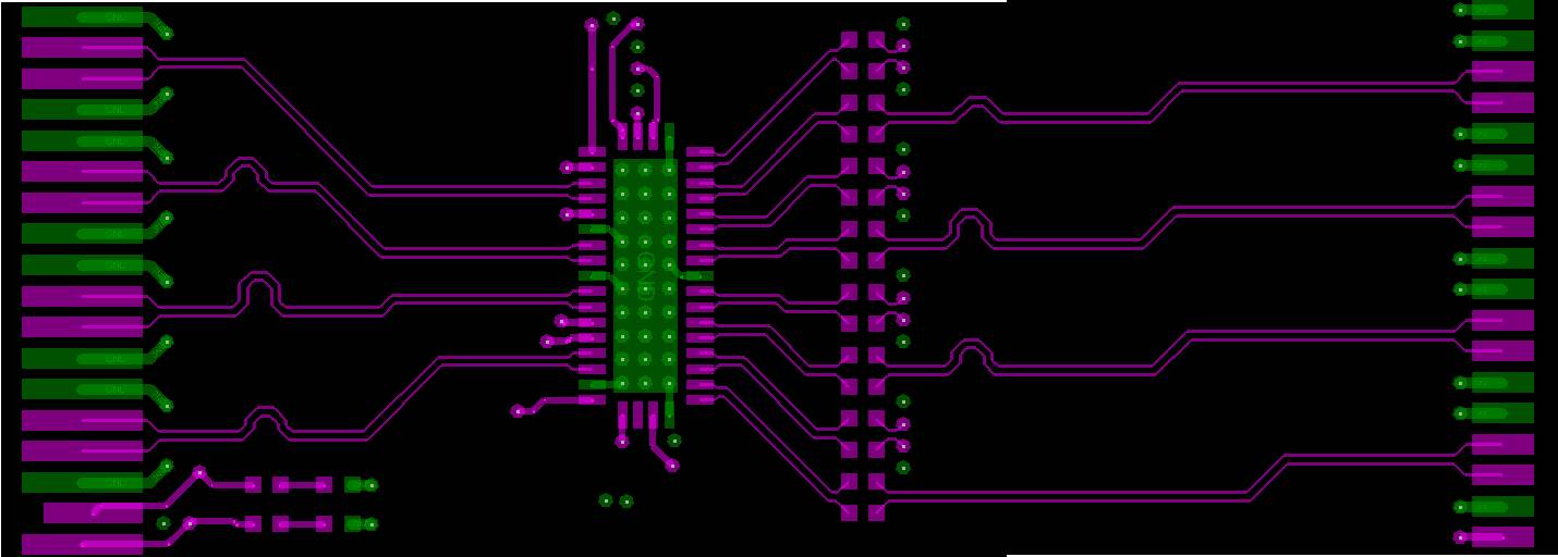
#FIG_LHY_PRX_WNB shows DS320PR421 layout example.
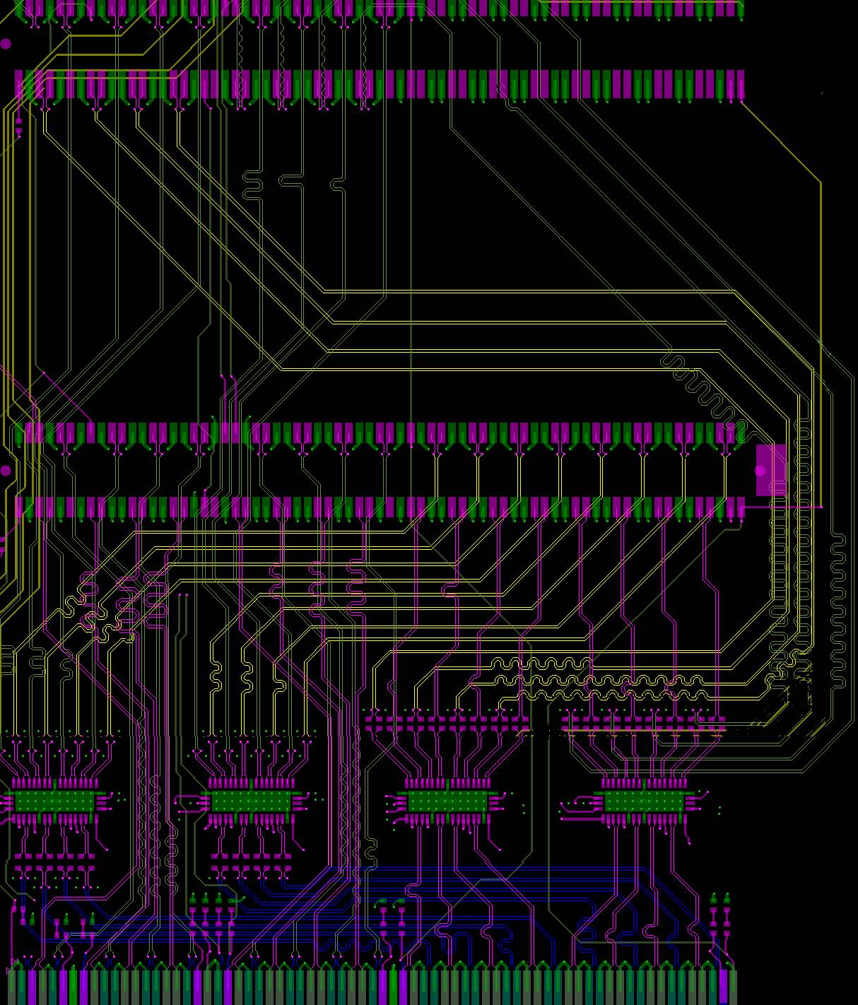
 Figure 11-1 DS320PR421 layout example#SLASE741248 shows a layout illustration where two DS320PR412 and two DS320PR421 are used to switch 8 lanes between two PCIe
slots.
 Figure 11-2 Layout example for PCIe lane muxing
application
 Figure 11-1 DS320PR421 layout example
 Figure 11-2 Layout example for PCIe lane muxing
application