ZHCSKE7B February 2017 – October 2019 DS250DF210
PRODUCTION DATA.
- 1 特性
- 2 应用
- 3 说明
- 4 修订历史记录
- 5 说明 (续)
- 6 Pin Configuration and Functions
-
7 Specifications
- 7.1 Absolute Maximum Ratings
- 7.2 ESD Ratings
- 7.3 Recommended Operating Conditions
- 7.4 Thermal Information
- 7.5 Electrical Characteristics
- 7.6 Timing Requirements, Retimer Jitter Specifications
- 7.7 Timing Requirements, Retimer Specifications
- 7.8 Timing Requirements, Recommended Calibration Clock Specifications
- 7.9 Recommended SMBus Switching Characteristics (Slave Mode)
- 7.10 Recommended SMBus Switching Characteristics (Master Mode)
- 7.11 Typical Characteristics
-
8 Detailed Description
- 8.1 Overview
- 8.2 Functional Block Diagram
- 8.3
Feature Description
- 8.3.1 Device Data Path Operation
- 8.3.2 Signal Detect
- 8.3.3 Continuous Time Linear Equalizer (CTLE)
- 8.3.4 Variable Gain Amplifier (VGA)
- 8.3.5 Cross-Point Switch
- 8.3.6 Decision Feedback Equalizer (DFE)
- 8.3.7 Clock and Data Recovery (CDR)
- 8.3.8 Calibration Clock
- 8.3.9 Differential Driver With FIR Filter
- 8.3.10 Debug Features
- 8.3.11 Interrupt Signals
- 8.4 Device Functional Modes
- 8.5 Programming
- 8.6 Register Maps
- 9 Application and Implementation
- 10Power Supply Recommendations
- 11Layout
- 12器件和文档支持
- 13机械、封装和可订购信息
8.3.9 Differential Driver With FIR Filter
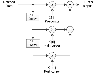
The DS250DF210 output driver has a three-tap finite impulse response (FIR) filter which allows for precursor and postcursor equalization to compensate for a wide variety of output channel media. The filter consists of a weighted sum of three consecutive retimed bits as shown in the following diagram. C[0] can take on values in the range [-31, +31]. C[-1] and C[+1] can take on values in the range [-15, 15].
 Figure 7. FIR Filter Functional Model
 When using the FIR filter, it is important to abide by the following general rules:
- |C[-1]| + |C[0]| + |C[+1]| ≤ 31; the FIR tap coefficients absolute sum must be less or equal to 31
- sgn(C[-1]) = sgn(C[+1]) ≠ sgn(C[0]), for high-pass filter effect; the sign for the precursor or postcursor tap must be different from main-cursor tap to realize boost effect
- sgn(C[-1]) = sgn(C[+1]) = sgn(C[0]), for low-pass filter effect; the sign for the precursor or postcursor tap must be equal to the main-cursor tap to realize attenuation effect
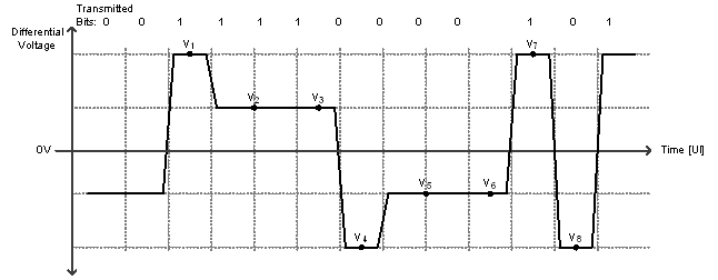
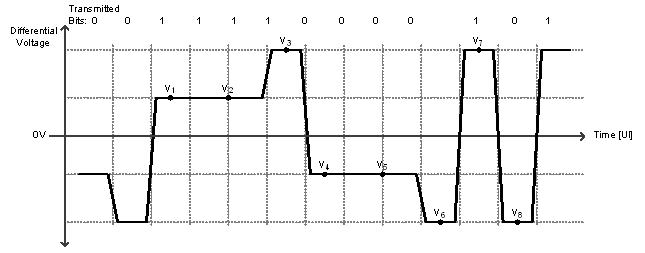
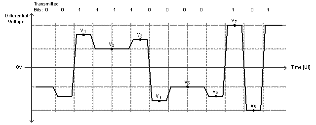
The FIR filter is used to predistort the transmitted waveform in order to compensate for frequency-dependant loss in the output channel. The most common way of predistorting the signal is to accentuate the transitions and de-emphasize the non-transitions. The bit before a transition is accentuated via the precursor tap, and the bit after the transition is accentuated through the postcursor tap. The figures below give a conceptual illustration of how the FIR filter affects the output waveform. The following characteristics can be derived from the example waveforms.
- VODpk-pk= v7 - v8
- VODlow-frequency = v2 - v5
- RpredB = 20 * log10 (v3 ⁄v2 )
- RpstdB = 20 * log10 (v1 ⁄v2 )
 Figure 8. Conceptual FIR Waveform With Postcursor Only
  Figure 9. Conceptual FIR Waveform With Precursor Only
  Figure 10. Conceptual FIR Waveform With Both Precursor and Postcursor