ZHCSKE7B February 2017 – October 2019 DS250DF210
PRODUCTION DATA.
- 1 特性
- 2 应用
- 3 说明
- 4 修订历史记录
- 5 说明 (续)
- 6 Pin Configuration and Functions
-
7 Specifications
- 7.1 Absolute Maximum Ratings
- 7.2 ESD Ratings
- 7.3 Recommended Operating Conditions
- 7.4 Thermal Information
- 7.5 Electrical Characteristics
- 7.6 Timing Requirements, Retimer Jitter Specifications
- 7.7 Timing Requirements, Retimer Specifications
- 7.8 Timing Requirements, Recommended Calibration Clock Specifications
- 7.9 Recommended SMBus Switching Characteristics (Slave Mode)
- 7.10 Recommended SMBus Switching Characteristics (Master Mode)
- 7.11 Typical Characteristics
-
8 Detailed Description
- 8.1 Overview
- 8.2 Functional Block Diagram
- 8.3
Feature Description
- 8.3.1 Device Data Path Operation
- 8.3.2 Signal Detect
- 8.3.3 Continuous Time Linear Equalizer (CTLE)
- 8.3.4 Variable Gain Amplifier (VGA)
- 8.3.5 Cross-Point Switch
- 8.3.6 Decision Feedback Equalizer (DFE)
- 8.3.7 Clock and Data Recovery (CDR)
- 8.3.8 Calibration Clock
- 8.3.9 Differential Driver With FIR Filter
- 8.3.10 Debug Features
- 8.3.11 Interrupt Signals
- 8.4 Device Functional Modes
- 8.5 Programming
- 8.6 Register Maps
- 9 Application and Implementation
- 10Power Supply Recommendations
- 11Layout
- 12器件和文档支持
- 13机械、封装和可订购信息
9.2.2 Active Cable Applications
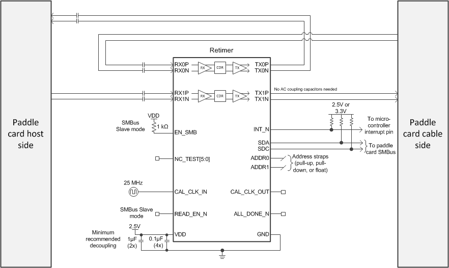
The DS250DF210 has strong equalization capabilities that allow it to recover data over long or thin-gauge copper cables. A single DS250DF210 can be used on a SFP28 paddle card to create a full-active cable assembly which is longer or thinner than passive cables.
Figure 18 illustrates this configuration, Figure 19 shows an example simplified schematic for a full-active cable application.
 Figure 18. Active Cable Application Block Diagram
  Figure 19. Full-Active Cable Application Schematic