ZHCSME1C August 2018 – June 2021 DS250DF230
PRODUCTION DATA
- 1 特性
- 2 应用
- 3 说明
- 4 Revision History
- 5 说明(续)
- 6 Pin Configuration and Functions
- 7 Specifications
-
8 Detailed Description
- 8.1 Overview
- 8.2 Functional Block Diagram
- 8.3
Feature Description
- 8.3.1 Device Data Path Operation
- 8.3.2 Signal Detect
- 8.3.3 Continuous Time Linear Equalizer (CTLE)
- 8.3.4 Variable Gain Amplifier (VGA)
- 8.3.5 Cross-Point Switch
- 8.3.6 Decision Feedback Equalizer (DFE)
- 8.3.7 Clock and Data Recovery (CDR)
- 8.3.8 Calibration Clock
- 8.3.9 Differential Driver With FIR Filter
- 8.3.10 Debug Features
- 8.3.11 Interrupt Signals
- 8.4 Device Functional Modes
- 8.5 Programming
- 8.6 Register Maps
- 9 Application and Implementation
- 10Power Supply Recommendations
- 11Layout
- 12Device and Documentation Support
- 13Electrostatic Discharge Caution
- 14术语表
- 15Mechanical, Packaging, and Orderable Information
封装选项
机械数据 (封装 | 引脚)
散热焊盘机械数据 (封装 | 引脚)
- RTV|32
订购信息
8.3.9.1 Setting the Output VOD, Pre-Cursor, and Post-Cursor Equalization
The output differential voltage (VOD), pre-cursor, and post-cursor equalization of the driver is controlled by manipulating the FIR tap settings. The main cursor tap is the primary knob for amplitude adjustment. The pre- and post-cursor FIR tap settings can then be adjusted to provide equalization. To maintain a constant peak-to-peak VOD, the user must adjust the main cursor tap value relative to the pre- and post-cursor tap changes so as to maintain a constant absolute sum of the FIR tap values. Table 8-2 shows various settings for VOD settings ranging from 350 mVpp to 1195 mVpp (typical). Note that the output peak-to-peak amplitude is a function of the sum of the absolute values of the taps, whereas the low-frequency amplitude is purely a function of the main-cursor value.
| FIR SETTINGS | Peak-to Peak VOD(V) | RPRE(dB) | RPST(dB) | ||
|---|---|---|---|---|---|
| PRE-CURSOR: REG_0x3E[6:0] | MAIN-CURSOR: REG_0x3D[6:0] | POST-CURSOR: REG_0x3F[6:0] | |||
| 0 | +3 | 0 | 0.350 | NA | NA |
| 0 | +4 | 0 | 0.392 | NA | NA |
| 0 | +5 | 0 | 0.436 | NA | NA |
| 0 | +6 | 0 | 0.482 | NA | NA |
| 0 | +7 | 0 | 0.524 | NA | NA |
| 0 | +8 | 0 | 0.562 | NA | NA |
| 0 | +9 | 0 | 0.602 | NA | NA |
| 0 | +10 | 0 | 0.638 | NA | NA |
| 0 | +11 | 0 | 0.678 | NA | NA |
| 0 | +12 | 0 | 0.710 | NA | NA |
| 0 | +13 | 0 | 0.748 | NA | NA |
| 0 | +14 | 0 | 0.782 | NA | NA |
| 0 | +15 | 0 | 0.816 | NA | NA |
| 0 | +16 | 0 | 0.846 | NA | NA |
| 0 | +17 | 0 | 0.880 | NA | NA |
| 0 | +18 | 0 | 0.910 | NA | NA |
| 0 | +19 | 0 | 0.944 | NA | NA |
| 0 | +20 | 0 | 0.968 | NA | NA |
| 0 | +21 | 0 | 0.998 | NA | NA |
| 0 | +22 | 0 | 1.028 | NA | NA |
| 0 | +23 | 0 | 1.056 | NA | NA |
| 0 | +24 | 0 | 1.076 | NA | NA |
| 0 | +25 | 0 | 1.096 | NA | NA |
| 0 | +26 | 0 | 1.120 | NA | NA |
| 0 | +27 | 0 | 1.140 | NA | NA |
| 0 | +28 | 0 | 1.155 | NA | NA |
| 0 | +29 | 0 | 1.175 | NA | NA |
| 0 | +30 | 0 | 1.185 | NA | NA |
| 0 | +31 | 0 | 1.195 | NA | NA |
| 0 | +16 | –1 | 0.880 | NA | 2.0 |
| 0 | +15 | –2 | 0.880 | NA | 2.7 |
| 0 | +14 | –3 | 0.880 | NA | 3.4 |
| 0 | +13 | –4 | 0.880 | NA | 4.3 |
| 0 | +12 | –5 | 0.880 | NA | 5.4 |
| 0 | +11 | –6 | 0.880 | NA | 6.7 |
| 0 | +10 | –7 | 0.880 | NA | 8.4 |
| 0 | +9 | –8 | 0.880 | NA | 11 |
| -1 | +16 | 0 | 0.880 | 0.7 | NA |
| -2 | +15 | 0 | 0.880 | 1.5 | NA |
| -3 | +14 | 0 | 0.880 | 2.5 | NA |
| -4 | +13 | 0 | 0.880 | 3.5 | NA |
| 0 | +30 | –1 | 1.195 | NA | 0.6 |
| 0 | +29 | –2 | 1.195 | NA | 0.8 |
| 0 | +28 | –3 | 1.195 | NA | 1.1 |
| 0 | +27 | –4 | 1.195 | NA | 1.4 |
| 0 | +26 | –5 | 1.195 | NA | 1.8 |
| 0 | +25 | –6 | 1.195 | NA | 2.3 |
| 0 | +24 | –7 | 1.195 | NA | 2.8 |
| 0 | +23 | –8 | 1.195 | NA | 3.4 |
| 0 | +22 | –9 | 1.195 | NA | 4.1 |
| 0 | +21 | –10 | 1.195 | NA | 4.9 |
| 0 | +20 | –11 | 1.195 | NA | 5.9 |
| 0 | +19 | –12 | 1.195 | NA | 6.9 |
| -1 | +30 | 0 | 1.195 | 0.4 | NA |
| -2 | +29 | 0 | 1.195 | 0.6 | NA |
| -3 | +28 | 0 | 1.195 | 0.9 | NA |
| -4 | +27 | 0 | 1.195 | 1.3 | NA |
| -5 | +26 | 0 | 1.195 | 1.7 | NA |
| -6 | +25 | 0 | 1.195 | 2.1 | NA |
| -7 | +24 | 0 | 1.195 | 2.7 | NA |
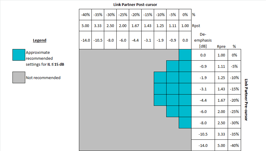
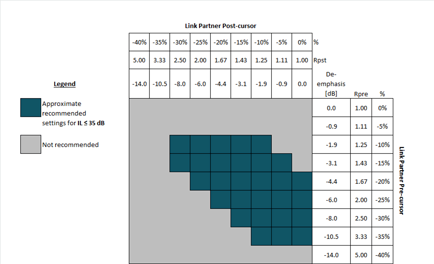
The recommended pre-cursor and post-cursor settings for a given channel will depend on the channel characteristics (mainly insertion loss) as well as the equalization capabilities of the downstream receiver. The DS250DF230 receiver, with its highly-capable CTLE and DFE, does not require a significant amount of pre- or post-cursor. The guidelines in Figure 8-5 through Figure 8-7 give general recommendations for pre- and post-cursor for different channel loss conditions. The insertion loss (IL) in these plots refers to the total loss between the link partner transmitter and the DS250DF230 receiver.
 Figure 8-5 Guideline for Link Partner FIR Settings When IL ≤ 15 dB
 Figure 8-6 Guideline for Link Partner FIR Settings When IL ≤ 25 dB
 Figure 8-7 Guideline for Link Partner FIR Settings When IL ≤ 35 dB