ZHCSME1C August 2018 – June 2021 DS250DF230
PRODUCTION DATA
- 1 特性
- 2 应用
- 3 说明
- 4 Revision History
- 5 说明(续)
- 6 Pin Configuration and Functions
- 7 Specifications
-
8 Detailed Description
- 8.1 Overview
- 8.2 Functional Block Diagram
- 8.3
Feature Description
- 8.3.1 Device Data Path Operation
- 8.3.2 Signal Detect
- 8.3.3 Continuous Time Linear Equalizer (CTLE)
- 8.3.4 Variable Gain Amplifier (VGA)
- 8.3.5 Cross-Point Switch
- 8.3.6 Decision Feedback Equalizer (DFE)
- 8.3.7 Clock and Data Recovery (CDR)
- 8.3.8 Calibration Clock
- 8.3.9 Differential Driver With FIR Filter
- 8.3.10 Debug Features
- 8.3.11 Interrupt Signals
- 8.4 Device Functional Modes
- 8.5 Programming
- 8.6 Register Maps
- 9 Application and Implementation
- 10Power Supply Recommendations
- 11Layout
- 12Device and Documentation Support
- 13Electrostatic Discharge Caution
- 14术语表
- 15Mechanical, Packaging, and Orderable Information
封装选项
机械数据 (封装 | 引脚)
散热焊盘机械数据 (封装 | 引脚)
- RTV|32
订购信息
9.2.1 Front-Port Jitter Cleaning Applications
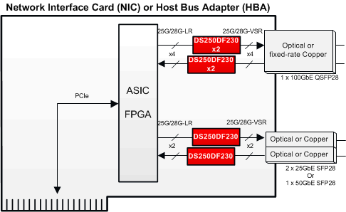
The DS250DF230 has strong equalization capabilities that allow it to equalize insertion loss, reduce jitter, and extend the reach of front-port interfaces. Two pieces DS250DF230 can be used to support all four egress channels for a 100GbE port. Another two pieces DS250DF230 can be used to support all four ingress channels for the same 100GbE ports. Alternatively, a single DS250DF230 can be used to support all egress channels for two 25GbE ports, and another DS250DF230 can be used to support all two ingress channels for the same four 25GbE ports.
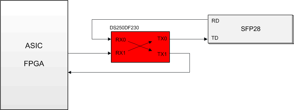
A flow-through pinout for the high-speed signals on DS250DF230 makes placement and routing easy for unidirectional application. By using the 2x2 cross point inside the device, DS250DF230 can also be configured for Figure 9-2, where one single device supports both egress and ingress channels.
 Figure 9-2 Bidirectional Application
For applications which require IEEE802.3 100GBASE-CR4 or 25GBASE-CR auto-negotiation and link training, a linear repeater device such as the DS280BR820 (or similar) is recommended.
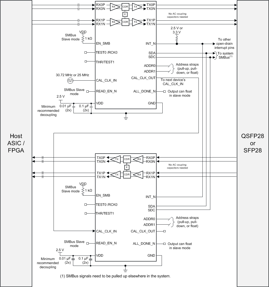
Figure 9-3 shows this configuration, and Figure 9-4 shows an example simplified schematic for a typical front-port application.
 Figure 9-3 Front-Port
Application Block Diagram
 Figure 9-4 Front-Port Application Schematic