ZHCSME1C August 2018 – June 2021 DS250DF230
PRODUCTION DATA
- 1 特性
- 2 应用
- 3 说明
- 4 Revision History
- 5 说明(续)
- 6 Pin Configuration and Functions
- 7 Specifications
-
8 Detailed Description
- 8.1 Overview
- 8.2 Functional Block Diagram
- 8.3
Feature Description
- 8.3.1 Device Data Path Operation
- 8.3.2 Signal Detect
- 8.3.3 Continuous Time Linear Equalizer (CTLE)
- 8.3.4 Variable Gain Amplifier (VGA)
- 8.3.5 Cross-Point Switch
- 8.3.6 Decision Feedback Equalizer (DFE)
- 8.3.7 Clock and Data Recovery (CDR)
- 8.3.8 Calibration Clock
- 8.3.9 Differential Driver With FIR Filter
- 8.3.10 Debug Features
- 8.3.11 Interrupt Signals
- 8.4 Device Functional Modes
- 8.5 Programming
- 8.6 Register Maps
- 9 Application and Implementation
- 10Power Supply Recommendations
- 11Layout
- 12Device and Documentation Support
- 13Electrostatic Discharge Caution
- 14术语表
- 15Mechanical, Packaging, and Orderable Information
封装选项
机械数据 (封装 | 引脚)
散热焊盘机械数据 (封装 | 引脚)
- RTV|32
订购信息
6 Pin Configuration and Functions
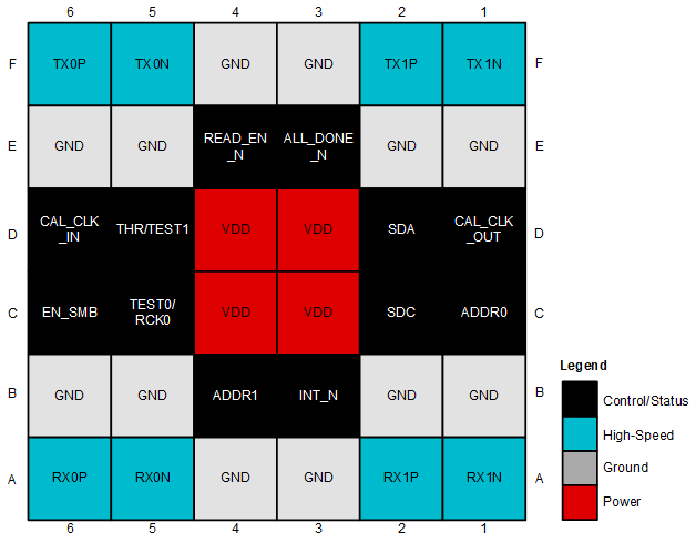
 Figure 6-1 ZLS
Package36-Pin NFBGATop View
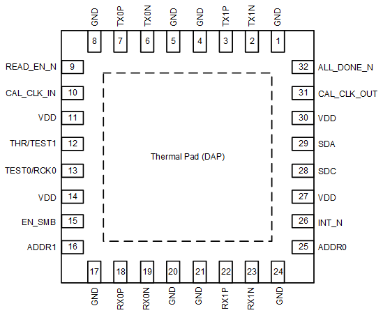
 Figure 6-2 RTV
Package32-Pin QFNTop View
Figure 6-2 RTV
Package32-Pin QFNTop ViewTable 6-1 Pin Functions
| PIN | TYPE | INTERNAL PULL-UP/ PULL-DOWN |
DESCRIPTION | ||
|---|---|---|---|---|---|
| NAME | NFBGA | QFN | |||
| HIGH-SPEED DIFFERENTIAL I/Os | |||||
| RX0P | A6 | 18 | Input | None | Inverting and noninverting differential inputs to the equalizer. An on-chip, 100-Ω termination resistor connects RXP to RXN. These inputs must be AC-coupled. |
| RX0N | A5 | 19 | Input | None | |
| RX1P | A2 | 22 | Input | None | Inverting and noninverting differential inputs to the equalizer. An on-chip, 100-Ω termination resistor connects RXP to RXN. These inputs must be AC-coupled. |
| RX1N | A1 | 23 | Input | None | |
| TX0P | F6 | 7 | Output | None | Inverting and noninverting 50Ω driver outputs. These outputs must be AC-coupled. |
| TX0N | F5 | 6 | Output | None | |
| TX1P | F2 | 3 | Output | None | Inverting and noninverting 50Ω driver outputs. These outputs must be AC-coupled. |
| TX1N | F1 | 2 | Output | None | |
| CALIBRATION CLOCK PINS | |||||
| CAL_CLK_IN | D6 | 10 | Input, 2.5V LVCMOS | None | 30.72-MHz (±100 PPM), 2.5-V single-ended clock from external oscillator. No stringent phase noise or jitter requirements on this clock. Also supports 25-MHz (±100 PPM) clock by programming the corresponding registers. |
| CAL_CLK_OUT | D1 | 31 | Output, 2.5V LVCMOS | None | 2.5-V buffered replica of calibration clock input (CAL_CLK_IN) for connecting multiple (up to 20 or more) devices in a daisy-chained fashion. |
| SYSTEM MANAGEMENT BUS (SMBus) PINS | |||||
| ADDR0 | C1 | 25 | Input, 4-level | None | 4-level strap pins used to set the SMBus address of
the device. The pin state is read on power-up. The multi-level nature of these pins
allows for 16 unique device addresses. The four strap options include: 0: 1 kΩ to GND R: 10 kΩ to GND F: Float 1: 1 kΩ to VDD Refer to Section 8.4.3 for more information. |
| ADDR1 | B4 | 16 | Input, 4-level | None | |
| EN_SMB | C6 | 15 | Input, 4-level | None | Four-level, 2.5-V input used to select between SMBus master mode
(float) and SMBus slave mode (high). The three defined levels are: R: 10 kΩ to GND - RESERVED, TI test mode F: Float - SMBus Master Mode (2.5-V/3.3-V SMBUS interface only) 1: 1 kΩ to VDD - SMBus Slave Mode |
| THR /TEST1 | D5 | 12 | Input, 4-level | None | Select the electrical voltage of SMBus interface. 2.5-V/3.3-V or
1.8-V: 1: 1 kΩ to VDD - 1.8-V SMBus interface F: Float - 1.8-V SMBus interface 0: 1 kΩ to GND - 2.5-V/3.3-V SMBus interface In TI test mode (EN_SMB = 10k Ohm to GND), this is reserved TI test pin. |
| SDA | D2 | 29 | I/O, Open Drain | None | SMBus data input / open-drain output. External 2-kΩ to 5-kΩ pullup resistor is required as per SMBus interface standard. This pin is 3.3-V tolerant. |
| SDC | C2 | 28 | I/O, Open Drain | None | SMBus clock input / open-drain clock output. External 2-kΩ to 5-kΩ pullup resistor is required as per SMBus interface standard. This pin is 3.3-V tolerant. |
| SMBus MASTER MODE PINS | |||||
| ALL_DONE_N | E3 | 32 | Output, 2.5-V LVCMOS | None | Indicates the completion of a valid EEPROM register load
operation when in SMBus Master Mode (EN_SMB=Float): High = External EEPROM load failed or incomplete Low = External EEPROM load successful and complete When in SMBus slave mode (EN_SMB=1), this output reflects the status of the READ_EN_N input. |
| READ_EN_N | E4 | 9 | Input, 3.3-V LVCMOS | Weak pullup to VDD | SMBus Master Mode (EN_SMB=Float): When asserted low, initiates
the SMBus master mode EEPROM read function. Once EEPROM read is complete (indicated
by assertion of ALL_DONE_N low), this pin can be held low for normal device
operation. SMBus Slave Mode (EN_SMB=1): When asserted low, this causes the device to be held in reset (SMBus state machine reset and register reset). This pin must be pulled high or left floating for normal operation in SMBus Slave Mode. This pin is 3.3-V tolerant. |
| MISCELLANEOUS PINS | |||||
| INT_N | B3 | 26 | Output, Open-Drain | None | Open-drain, 3.3-V tolerant active-low interrupt output. It pulls low when an interrupt occurs. The events which trigger an interrupt are programmable through SMBus registers. This pin can be connected in a wired-OR fashion with other device's interrupt pin. A single pullup resistor in the 2-kΩ to 5-kΩ range is adequate for the entire INT_N net. |
| TEST0 /RCK0 | C5 | 13 | I/O, 2.5-V LVCMOS | None | In TI test mode (EN_SMB = 10k Ohm to GND), this is reserved TI
test pin. During normal (non-test-mode) operation, this pin is configured as input by default and therefore is not affected by the presence of a signal. This pin may be left floating, tied to GND, or connected to a 2.5-V (max) output. This pin can be configured to offer the recovered clock for CH0 by programming the corresponding registers. The signal is 2.5-V LVCMOS. |
| POWER | |||||
| VDD | C3, C4,D3, D4 | 11, 14, 27, 30 | Power | None | Power supply, VDD = 2.5 V ±5%. TI recommends connecting at least four de-coupling capacitors between the Retimer VDD plane and GND as close to the Retimer as possible. For example, two 0.1-µF capacitors, and two 0.01-µF capacitors directly beneath the device or as close to the VDD pins as possible. The VDD pins on this device must be connected through a low-resistance path to the board VDD plane. |
| GND | A3, A4,B1, B2,B5, B6,E1, E2,E5, E6,F3, F4 | 1, 4, 5, 8, 17, 20, 21, 24 | Power | None | Ground reference. The GND pins on this device must be connected through a low-resistance path to the board GND plane. |
| DAP | — | DAP | Power | None | DAP is the exposed pad at the bottom of the RTV package. The exposed pad should be connected to the GND plane through a 3x3 via array. |