ZHCSKG1C November 2015 – October 2019 DS280BR810
PRODUCTION DATA.
- 1 特性
- 2 应用
- 3 说明
- 4 修订历史记录
- 5 Pin Configuration and Functions
- 6 Specifications
- 7 Detailed Description
- 8 Application and Implementation
- 9 Power Supply Recommendations
- 10Layout
- 11器件和文档支持
- 12机械、封装和可订购信息
10.2 Layout Example
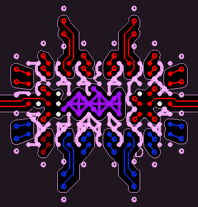
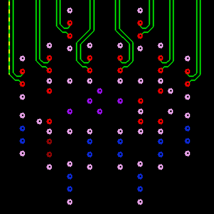
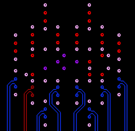
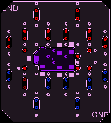
The following example layout demonstrates how all signals can be escaped from the BGA array using stripline routing on a generic 28-layer stackup. This example layout assumes the following:
- Trace width: 0.127 mm (5 mil)
- Trace edge-to-edge spacing: 0.152 mm (6 mil)
- VIA finished hole size (diameter): 0.203 mm (8 mil)
- VIA drilled hole size: 0.254 mm (10 mil)
- VIA-to-VIA spacing: 1.0 mm (39 mil), to enhance PCB manufacturability
- No VIA-in-pad used
Note that many other escape routing options exist using different trace width and spacing combinations. The optimum trace width and spacing will depend on the PCB material, PCB routing density, and other factors. Microstrip escape routing is also possible and may be preferable in some application scenarios, including front-port applications.
 Figure 29. Top Layer
  Figure 31. Internal Signal Layer 2
  Figure 30. Internal Signal Layer 1
  Figure 32. Bottom Layer