ZHCSKG2B September   2016  – October 2019 DS280BR820

PRODUCTION DATA.  

  1. 特性
  2. 应用
  3. 说明
    1.     简化电路原理图
  4. 修订历史记录
  5. Pin Configuration and Functions
    1.     Pin Functions
  6. Specifications
    1. 6.1 Absolute Maximum Ratings
    2. 6.2 ESD Ratings
    3. 6.3 Recommended Operating Conditions
    4. 6.4 Thermal Information
    5. 6.5 Electrical Characteristics
    6. 6.6 Electrical Characteristics – Serial Management Bus Interface
    7. 6.7 Timing Requirements – Serial Management Bus Interface
    8. 6.8 Typical Characteristics
  7. Detailed Description
    1. 7.1 Overview
    2. 7.2 Functional Block Diagram
    3. 7.3 Feature Description
      1. 7.3.1 Device Data Path Operation
      2. 7.3.2 AC-Coupled Receiver Inputs
      3. 7.3.3 Signal Detect
      4. 7.3.4 2-Stage CTLE
      5. 7.3.5 Driver DC Gain Control
      6. 7.3.6 FIR Filter (Limiting Mode)
      7. 7.3.7 Configurable SMBus Address
    4. 7.4 Device Functional Modes
      1. 7.4.1 SMBus Slave Mode Configuration
      2. 7.4.2 SMBus Master Mode Configuration (EEPROM Self Load)
    5. 7.5 Programming
      1. 7.5.1 Transfer of Data with the SMBus Interface
    6. 7.6 Register Maps
      1. 7.6.1 Register Types: Global, Shared, and Channel
      2. 7.6.2 Global Registers: Channel Selection and ID Information
        1. Table 2. Global Register Map
      3. 7.6.3 Shared Registers
        1. Table 3. Shared Register Map
      4. 7.6.4 Channel Registers
        1. Table 4. Channel Register Map
  8. Application and Implementation
    1. 8.1 Application Information
    2. 8.2 Typical Applications
      1. 8.2.1 Backplane and Mid-Plane Reach Extension
        1. 8.2.1.1 Design Requirements
        2. 8.2.1.2 Detailed Design Procedure
      2. 8.2.2 Front-Port Applications
        1. 8.2.2.1 Design Requirements
        2. 8.2.2.2 Detailed Design Procedure
      3. 8.2.3 Application Curves
        1. 8.2.3.1 Pattern Generator Characteristics
        2. 8.2.3.2 Equalizing Moderate Pre-Channel Loss
        3. 8.2.3.3 Equalizing High Pre-Channel Loss
        4. 8.2.3.4 Equalizing High Pre-Channel Loss and Moderate Post-Channel Loss
        5. 8.2.3.5 Output in FIR Limiting Mode with 16T Pattern
    3. 8.3 Initialization Set Up
  9. Power Supply Recommendations
  10. 10Layout
    1. 10.1 Layout Guidelines
    2. 10.2 Layout Examples
      1. 10.2.1 Stripline Example
      2. 10.2.2 Microstrip Example
  11. 11器件和文档支持
    1. 11.1 文档支持
      1. 11.1.1 相关文档
    2. 11.2 接收文档更新通知
    3. 11.3 商标
    4. 11.4 静电放电警告
    5. 11.5 Glossary

封装选项

机械数据 (封装 | 引脚)
散热焊盘机械数据 (封装 | 引脚)
订购信息

Equalizing Moderate Pre-Channel Loss

This example application result demonstrates the DS280BR820 equalizing for pre-channel insertion loss introduced by an FR4 channel.

DS280BR820 AppData_preChan.gifFigure 18. 5 in input Channel and Minimal Output Channel Test Setup
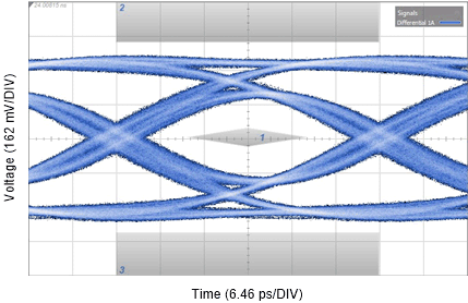
DS280BR820 AppData_Pre5in_25G.gifFigure 19. 25.78125 Gbps CAUI-4 Eye Mask with 5 in Input Channel and Minimal Output Channel
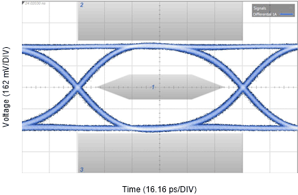
DS280BR820 AppData_Pre5in_10G.gifFigure 20. 10.3125 Gbps nPPI Eye Mask with 5 in Input Channel and Minimal Output Channel

Table 6. Settings and Measurements for CAUI-4 and nPPI with 5 in Input Channel and Minimal Output Channel

25.78125 Gbps (CAUI-4) 10.3125 Gbps (nPPI)
Transmission Line 1 5 in 5 mil FR4 + 8 in SMA cable 5 in 5 mil FR4 + 8 in SMA cable
DS280BR820 Rx Channel Loss 14 dB @ 12.9 GHz 6 dB @ 5.2 GHz
DS280BR820 Tx Channel Loss 4.5 dB @ 12.9 GHz 2 dB @ 5.2 GHz
EQ BST1 3 3
EQ BST2 0 0
EQ BW 3 3
VOD 3 2
EQ DC Gain Mode Low Low
Total Jitter @ 1E-15 11.9 psP-P 13.0 psP-P
Differential Eye Height @ 1E-15 338 mVP-P 544 mVP-P
Mask violations 0 0