ZHCSKG3B September 2016 – February 2024 DS280DF810
PRODUCTION DATA
- 1
- 1 特性
- 2 应用
- 3 说明
- 4 Pin Configuration and Functions
-
5 Specifications
- 5.1 Absolute Maximum Ratings
- 5.2 ESD Ratings
- 5.3 Recommended Operating Conditions
- 5.4 Thermal Information
- 5.5 Electrical Characteristics
- 5.6 Timing Requirements, Retimer Jitter Specifications
- 5.7 Timing Requirements, Retimer Specifications
- 5.8 Timing Requirements, Recommended Calibration Clock Specifications
- 5.9 Recommended SMBus Switching Characteristics (Target Mode)
- 5.10 Recommended SMBus Switching Characteristics (Controller Mode)
- 5.11 Typical Characteristics
-
6 Detailed Description
- 6.1 Overview
- 6.2 Functional Block Diagram
- 6.3
Feature Description
- 6.3.1
Device Data Path Operation
- 6.3.1.1 AC-Coupled Receiver and Transmitter
- 6.3.1.2 Signal Detect
- 6.3.1.3 Continuous Time Linear Equalizer (CTLE)
- 6.3.1.4 Variable Gain Amplifier (VGA)
- 6.3.1.5 2x2 Cross-Point Switch
- 6.3.1.6 Decision Feedback Equalizer (DFE)
- 6.3.1.7 Clock and Data Recovery (CDR)
- 6.3.1.8 Calibration Clock
- 6.3.1.9 Differential Driver with FIR Filter
- 6.3.2 Debug Features
- 6.3.1
Device Data Path Operation
- 6.4 Device Functional Modes
- 6.5 Programming
- 6.6 Register Maps
- 7 Application and Implementation
- 8 Device and Documentation Support
- 9 Revision History
- 10Mechanical, Packaging, and Orderable Information
封装选项
请参考 PDF 数据表获取器件具体的封装图。
机械数据 (封装 | 引脚)
- ABW|135
- ABV|135
散热焊盘机械数据 (封装 | 引脚)
订购信息
7.2.3 Application Curves
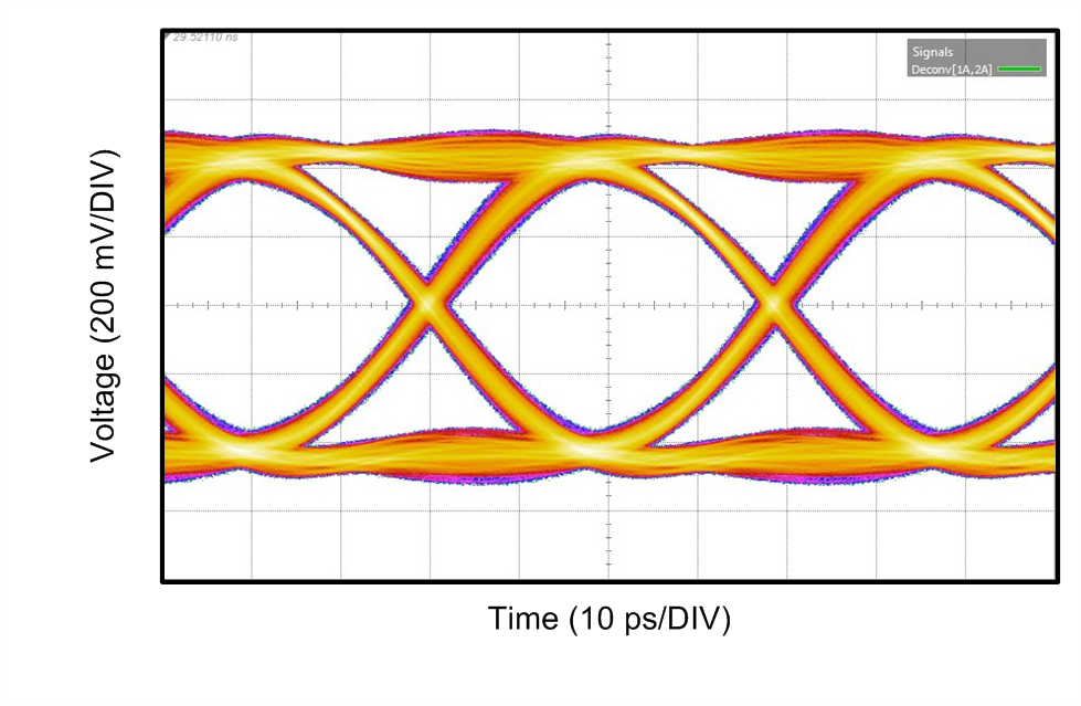
 Figure 7-6 DS280DF810 Operating at 25.78125Gbps
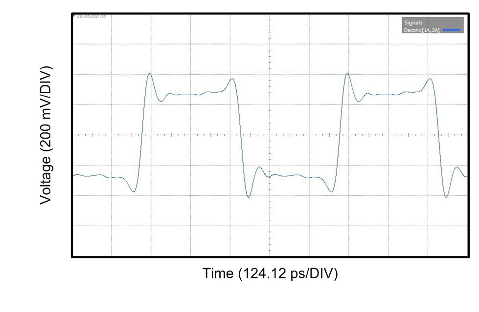
 Figure 7-7 DS280DF810 FIR Transmit Equalization while Operating at 25.78125Gbps
Figure 7-6 shows a typical output eye diagram for the DS280DF810 operating at 25.78125Gbps with PRBS9 pattern using FIR main-cursor of +18, pre-cursor of -1 and post-cursor of +2. All other device settings are left at default.
Figure 7-7 shows an example of DS280DF810 FIR transmit equalization while operating at 25.78125Gbps. In this example, the Tx FIR filter main-cursor is set to +15, post-cursor to -3 and pre-cursor to -3. An 8T pattern is used to evaluate the FIR filter, which consists of 0xFF00. All other device settings are left at default.