-
DS80PCI102 2.5-Gbps / 5.0-Gbps / 8.0-Gbps 1-Lane PCI-Express Repeater With Equalization and De-Emphasis
- 1 Features
- 2 Applications
- 3 Description
- 4 Revision History
- 5 Pin Configuration and Functions
- 6 Specifications
- 7 Detailed Description
- 8 Application and Implementation
- 9 Power Supply Recommendations
- 10Layout
- 11Device and Documentation Support
- 12Mechanical, Packaging, and Orderable Information
- IMPORTANT NOTICE
DS80PCI102 2.5-Gbps / 5.0-Gbps / 8.0-Gbps 1-Lane PCI-Express Repeater With Equalization and De-Emphasis
1 Features
- Comprehensive Family, Proven System Interoperability
-
DS80PCI102: x1 PCIe
Gen-1, Gen-2, and Gen-3 - DS80PCI402: x4 PCIe
Gen-1, Gen-2, and Gen-3 - DS80PCI800: x8/x16 PCIe
Gen-1, Gen-2, and Gen-3
-
DS80PCI102: x1 PCIe
- Automatic Rate-Detect and Adaptation to
Gen-1, Gen-2, and Gen-3 Speeds - Seamless Support for Gen-3 Transmit FIR Handshake
- Receiver EQ (up to 36 dB), Transmit De-Emphasis (up to -12 dB)
- Adjustable Transmit VOD: 0.7 to 1.3 Vp-p (Pin Mode)
- 0.2 UI of Residual Deterministic Jitter at 8 Gbps After 40 Inches of FR4 or 10 m 30-awg PCIe Cable
- Low Power Dissipation With Ability to Turn Off Unused Channels: 65 mW/Channel
- Automatic Receiver Detect (Hot-Plug)
- Multiple Configuration Modes: Pins/SMBus/Direct-EEPROM Load
- Flow-Thru Pinout in 4-mm × 4-mm 24-Pin Leadless WQFN Package
- Single Supply Voltage: 2.5 V or 3.3 V (Selectable)
- ±5-kV HBM ESD Rating
- −40°C to 85°C Operating Temperature Range
2 Applications
PCI Express Gen-1, Gen-2, and Gen-3
3 Description
The DS80PCI102 is a low-power, 1-lane repeater with 4-stage input equalization, and an output de-emphasis driver to enhance the reach of PCI-Express serial links in board-to-board or cable interconnects. The device is ideal for x1 PCI-Express configuration, and it automatically detects and adapts to Gen-1, Gen-2, and Gen-3 data rates for easy system upgrade.
DS80PCI102 offers programmable transmit de-emphasis (up to 12 dB), transmit VOD (up to
1300 mVp-p), and receive equalization (up to 36 dB) to enable longer distance transmission in lossy copper cables (10 meters or more), or backplanes (40 inches or more) with multiple connectors. The receiver can open an input eye that is completely closed due to inter-symbol interference (ISI) introduced by the interconnect medium.
The programmable settings can be applied easily through pins or software (SMBus/I2C), or can be loaded through an external EEPROM. When operating in the EEPROM mode, the configuration information is automatically loaded on power up, which eliminates the need for an external microprocessor or software driver.
Device Information(1)
| PART NUMBER | PACKAGE | BODY SIZE (NOM) |
|---|---|---|
| DS80PCI102 | WQFN (24) | 4.00 mm x 4.00 mm |
- For all available packages, see the orderable addendum at the end of the data sheet.
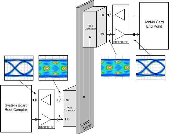
Typical Application Block Diagram

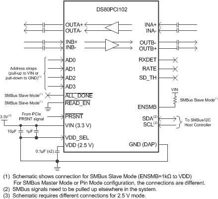
Simplified Schematic Diagram

4 Revision History
Changes from F Revision (October 2014) to G Revision
- Changed pin mapping for VIN and VDD to correct typoGo
- Added full SMBus-to-EEPROM table mappingGo
- Changed description of EEPROM bits to match corresponding SMBus register map description Go
- Changed location of CHB VOD in Table 7 to match correct location in EEPROM mapGo
- Changed address start and end numbers for Devices 0-3 to reflect correct bytes per device Go
- Changed EEPROM bit description to match the description in the corresponding SMBus register map Go
- Changed location of CHA VOD in Table 9 to match correct location in EEPROM map Go
- Added information in Register Map about register bits saved to EEPROM Go
Changes from E Revision (February 2013) to F Revision
- Added ESD Ratings table, Feature Description section, Device Functional Modes, Application and Implementation section, Power Supply Recommendations section, Layout section, Device and Documentation Support section, and Mechanical, Packaging, and Orderable Information sectionGo
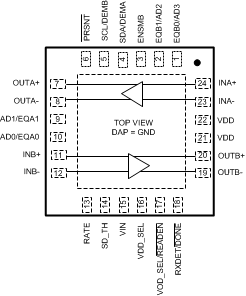
5 Pin Configuration and Functions

Pin Functions(1)(2)(3)(4)
| PIN | I/O, TYPE | DESCRIPTION | |||
|---|---|---|---|---|---|
| NAME | NO. | ||||
| DIFFERENTIAL HIGH SPEED I/O'S | |||||
| INA+, INA-, INB+, INB- |
24, 23 11, 12 |
I, CML | Inverting and noninverting differential inputs to the equalizer. A gated on-chip 50-Ω termination resistor connects INn+ to VDD and INn- to VDD depending on the state of RXDET. See Table 4
AC coupling required on high-speed I/O |
||
| OUTA+, OUTA-, OUTB+, OUTB- |
7, 8 20, 19 |
O, CML | Inverting and noninverting 50-Ω driver outputs with de-emphasis. Compatible with AC-coupled CML inputs. | ||
| CONTROL PINS — SHARED (LVCMOS) | |||||
| ENSMB | 3 | I, 4-LEVEL, LVCMOS | System management bus (SMBus) enable pin Tie 1 kΩ to VDD (2.5-V mode) or VIN (3.3-V mode) = Register access SMBus slave mode FLOAT = Read external EEPROM (master SMBUS mode) Tie 1 kΩ to GND = Pin mode |
||
| ENSMB = 1 (SMBus SLAVE MODE) | |||||
| SCL | 5 | I, 2-LEVEL, LVCMOS, O, open drain | In SMBus Slave Mode, this pin is the SMBus clock I/O. Clock input or open drain output. External 2-kΩ to 5-kΩ pullup resistor to VDD or VIN recommended as per SMBus interface standards.(5) |
||
| SDA | 4 | I, 2-LEVEL, LVCMOS, O, open drain | In both SMBus Modes, this pin is the SMBus data I/O. Data input or open drain output. External 2-kΩ to 5-kΩ pullup resistor to VDD or VIN recommended as per SMBus interface standards.(5) |
||
| AD0-AD3 | 10, 9, 2, 1 | I, 4-LEVEL, LVCMOS | SMBus Slave Address Inputs. In both SMBus Modes, these pins are the user set SMBus slave address inputs. External 1-kΩ pullup or pulldown recommended. |
||
| READEN | 17 | I, 2-LEVEL, LVCMOS | When in SMBus Slave Mode the READEN pin must be tied LOW for the AD[3:0] to be active. If this pin is tied HIGH or FLOAT, the device slave address is 0xB0. | ||
| ENSMB = FLOAT (SMBus MASTER MODE) | |||||
| SCL | 5 | I, 2-LEVEL, LVCMOS, O, open drain | Clock output when loading EEPROM configuration, reverting to SMBus clock input when EEPROM load is complete (DONE = 0). External 2-kΩ to 5-kΩ pullup resistor to VDD or VIN recommended as per SMBus interface standards.(5) |
||
| SDA | 4 | I, 2-LEVEL, LVCMOS, O, open drain | In both SMBus Modes, this pin is the SMBus data I/O. Data input or open drain output. External 2-kΩ to 5-kΩ pullup resistor to VDD or VIN recommended as per SMBus interface standards.(5) |
||
| AD0-AD3 | 10, 9, 2, 1 | I, 4-LEVEL, LVCMOS | SMBus Slave Address Inputs. In both SMBus Modes, these pins are the user set SMBus slave address inputs. External 1-kΩ pullup or pulldown recommended. |
||
| READEN | 17 | I, 2-LEVEL, LVCMOS | A logic low on this pin starts the load from the external EEPROM.(6)
Once EEPROM load is complete (DONE = 0), this pin functionality remains as READEN. It does not revert to an SD_TH input. |
||
| DONE | 18 | O, 2-LEVEL, LVCMOS | Valid register load status output HIGH = External EEPROM load failed or incomplete LOW = External EEPROM load passed |
||
| ENSMB = 0 (PIN MODE) | |||||
| EQA0, EQA1 EQB0, EQB1 |
10, 9 1, 2 |
I, 4-LEVEL, LVCMOS | EQA[1:0] and EQB[1:0] control the level of equalization on the input pins. The pins are active only when ENSMB is deasserted (LOW). When ENSMB goes high the SMBus registers provide independent control of each lane, and the EQA[1:0] and EQB[1:0] pins are converted to SMBUS AD[3:0] inputs. See Table 2. |
||
| DEMA, DEMB | 4, 5 | I, 4-LEVEL, LVCMOS | DEMA DEMB controls the level of de-emphasis. The DEMA/B pins are only active when ENSMB is deasserted (LOW). DEMA controls the A channel and DEMB controls the B channel. When ENSMB goes high the SMBus registers provide independent control of each channel and the DEM pins are converted to SMBUS SDA and SCL pins. See Table 3. |
||
| CONTROL PINS — BOTH PIN AND SMBUS MODES (LVCMOS) | |||||
| PRSNT | 6 | I, 2-LEVEL, LVCMOS | Cable Present Detect input. High when a cable is not present per PCIe Cabling Spec. 1.0. Puts part into low power mode. When LOW (normal operation) part is enabled. See Table 4. |
||
| VOD_SEL | 17 | I, 4-LEVEL, LVCMOS | VOD Select pin. See Table 3. | ||
| VDD_SEL | 16 | I, LVCMOS | Controls the internal regulator. FLOAT = 2.5-V mode Tie GND = 3.3-V mode See Figure 16. |
||
| RXDET | 18 | I, 4-LEVEL, LVCMOS | The RXDET pin controls the receiver detect function. Depending on the input level, a 50-Ω or > 50-kΩ termination to the power rail is enabled. See Table 4. |
||
| RATE | 13 | I, 4-LEVEL, LVCMOS | RATE control pin selects GEN 1,2 and GEN 3 operating modes. Tie 1 kΩ to GND = GEN 1,2 FLOAT = AUTO Rate Select of Gen1/2 and Gen3 with de-emphasis Tie 20 kΩ to GND = GEN 3 without de-emphasis Tied 1 kΩ to VDD = RESERVED |
||
| SD_TH | 14 | I, 4-LEVEL, LVCMOS | Controls the internal Signal Detect Threshold. See Table 5. |
||
| POWER | |||||
| VIN | 15 | Power | In 3.3-V mode, feed 3.3 V to VIN In 2.5-V mode, leave floating |
||
| VDD | 21, 22 | Power | Power supply pins 2.5-V mode, connect to 2.5-V supply 3.3-V mode, connect 0.1-µF capacitor to each VDD pin (output of LDO) |
||
| GND | DAP | Power | Ground pad (DAP - die attach pad). | ||