SNLS043H May 2000 – January 2016 DS90CR216A , DS90CR286A , DS90CR286A-Q1
PRODUCTION DATA.
- 1 Features
- 2 Applications
- 3 Description
- 4 Revision History
- 5 Pin Configuration and Functions
- 6 Specifications
- 7 Detailed Description
- 8 Application and Implementation
- 9 Power Supply Recommendations
- 10Layout
- 11Device and Documentation Support
- 12Mechanical, Packaging, and Orderable Information
7 Detailed Description
7.1 Overview
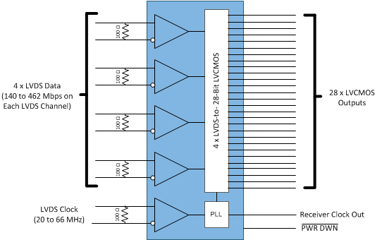
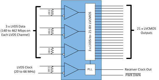
The DS90CR286A and DS90CR286A-Q1 are receivers that convert four LVDS (Low Voltage Differential Signaling) data streams into parallel 28 bits of LVCMOS data (24 bits of RGB and 4 bits of HSYNC, VSYNC, DE, and CNTL). The DS90CR216A is a receiver that converts three LVDS data streams back into parallel 21 bits of LVCMOS data (18 bits of RGB and 3 bits of HSYNC, VSYNC, and DE). An internal PLL locks to the incoming LVDS clock ranging from 20 to 66 MHz. The locked PLL ensures a stable clock to sample the output LVCMOS data on the Receiver Clock Out rising edge. These devices feature a PWR DWN pin to put the device into low power mode when there is no active input data.
7.2 Functional Block Diagrams


7.3 Feature Description
The DS90CR286A and DS90CR216A consist of several key blocks:
- LVDS Receivers
- Phase Locked Loop (PLL)
- Serial LVDS-to-Parallel LVCMOS Converter
- LVCMOS Drivers
7.3.1 LVDS Receivers
There are five differential LVDS inputs to the DS90CR286A and four differential LVDS inputs to the DS90CR216A. Four of the LVDS inputs contain serialized data originating from a 28-bit source transmitter. For the DS90CR216A, three of the LVDS inputs contain serialized data originating from a 21-bit source transmitter. The remaining LVDS input contains the LVDS clock associated with the data pairs.
7.3.1.1 LVDS Input Termination
The DS90CR286A and DS90CR216A require a single 100-Ω terminating resistor across the true and complement lines on each differential pair of the receiver input. To prevent reflections due to stubs, this resistor should be placed as close to the device input pins as possible. Figure 18 shows an example.
 Figure 18. LVDS Serialized Link Termination
7.3.2 Phase Locked Loop (PLL)
The Channel Link I devices use an internal PLL to recover the clock transmitted across the LVDS interface. The recovered clock is then used as a reference to determine the sampling position of the seven serial bits received per clock cycle. The width of each bit in the serialized LVDS data stream is one-seventh the clock period. Differential skew (Δt within one differential pair), interconnect skew (Δt of one differential pair to another) and clock jitter will all reduce the available window for sampling the LVDS serial data streams. Individual bypassing of each VCC to ground will minimize the noise passed on to the PLL, thus creating a low jitter LVDS clock to improve the overall jitter budget.
7.3.3 Serial LVDS-to-Parallel LVCMOS Converter
After the PLL locks to the incoming LVDS clock, the receiver deserializes each LVDS differential data pair into seven parallel LVCMOS data outputs per clock cycle. For the DS90CR286A, the LVDS data inputs map to LVCMOS outputs according to Figure 6. For the DS90CR216A, the LVDS data inputs map to LVCMOS outputs according to Figure 7.
7.3.4 LVCMOS Drivers
The LVCMOS outputs from the DS90CR286A and DS90CR216A are the deserialized parallel single-ended data from the serialized LVDS differential data pairs. Each LVCMOS output is clocked by the PLL and strobes on the RxCLKOUT rising edge. All unused DS90CR286A and DS90CR216A RxOUT outputs can be left floating.
7.4 Device Functional Modes
7.4.1 Power Down Mode
The DS90CR286A and DS90CR216A may be placed into a power down mode at any time by asserting the PWR DWN pin (active low). The DS90CR286A and DS90CR216A are also designed to protect themselves from accidental loss of power to either the transmitter or receiver. If power to the transmit board is lost, the receiver clocks (input and output) stop. The data outputs (RxOUT) retain the states they were in when the clocks stopped. When the receiver board loses power, the receiver inputs are shorted to VCC through an internal diode. Current is limited to 5 mA per input, thus avoiding the potential for latch-up when powering the device.