SNLS043H May 2000 – January 2016 DS90CR216A , DS90CR286A , DS90CR286A-Q1
PRODUCTION DATA.
- 1 Features
- 2 Applications
- 3 Description
- 4 Revision History
- 5 Pin Configuration and Functions
- 6 Specifications
- 7 Detailed Description
- 8 Application and Implementation
- 9 Power Supply Recommendations
- 10Layout
- 11Device and Documentation Support
- 12Mechanical, Packaging, and Orderable Information
6 Specifications
6.1 Absolute Maximum Ratings
see (1)(2)| MIN | MAX | UNIT | |||
|---|---|---|---|---|---|
| Supply voltage (VCC) | –0.3 | 4 | V | ||
| LVCMOS output voltage | –0.3 | (VCC + 0.3 V) | V | ||
| LVDS receiver input voltage | –0.3 | (VCC + 0.3 V) | V | ||
| Junction temperature | 150 | °C | |||
| Lead temperature (soldering, 4 sec) | 260 | °C | |||
| Storage temperature, Tstg | –65 | 150 | °C | ||
(1) Stresses beyond those listed under Absolute Maximum Ratings may cause permanent damage to the device. These are stress ratings only, which do not imply functional operation of the device at these or any other conditions beyond those indicated under Recommended Operating Conditions. Exposure to absolute-maximum-rated conditions for extended periods may affect device reliability.
(2) If Military/Aerospace specified devices are required, please contact the TI Sales Office/Distributors for availability and specifications.
6.2 ESD Ratings
| VALUE | UNIT | |||
|---|---|---|---|---|
| V(ESD) | Electrostatic discharge |
Human body model (HBM), per ANSI/ESDA/JEDEC JS-001(1) | ±7000 | V |
| Charged device model (CDM), per JEDEC specification JESD22-C101(2) | ±700 | |||
(1) JEDEC document JEP155 states that 500-V HBM allows safe manufacturing with a standard ESD control process.
(2) JEDEC document JEP157 states that 250-V CDM allows safe manufacturing with a standard ESD control process.
6.3 Recommended Operating Conditions
| MIN | NOM | MAX | UNIT | |
|---|---|---|---|---|
| Supply voltage (VCC) | 3.0 | 3.3 | 3.6 | V |
| Operating free air temperature (TA) | –40 | 25 | 85 | °C |
| Receiver input range | 0 | 2.4 | V | |
| Supply noise voltage (VNOISE) | 100 | mVPP |
6.4 Thermal Information
| THERMAL METRIC(1) | DS90CR286A/-Q1 | DS90CR216A | UNIT | |
|---|---|---|---|---|
| DGG (TSSOP) | DGG (TSSOP) | |||
| 56 PINS | 48 PINS | |||
| RθJA | Junction-to-ambient thermal resistance | 64.6 | 67.8 | °C/W |
| RθJC(top) | Junction-to-case (top) thermal resistance | 20.6 | 22.1 | °C/W |
| RθJB | Junction-to-board thermal resistance | 33.3 | 34.8 | °C/W |
| ψJT | Junction-to-top characterization parameter | 1.0 | 1.1 | °C/W |
| ψJB | Junction-to-board characterization parameter | 33.0 | 34.5 | °C/W |
(1) For more information about traditional and new thermal metrics, see the Semiconductor and IC Package Thermal Metrics application report, SPRA953.
6.5 Electrical Characteristics
Over recommended operating supply and temperature ranges unless otherwise specified.(1)(2)| PARAMETER | TEST CONDITIONS | MIN | TYP | MAX | UNIT | ||
|---|---|---|---|---|---|---|---|
| LVCMOS DC SPECIFICATIONS (For PWR DWN Pin) | |||||||
| VIH | High Level Input Voltage | 2 | VCC | V | |||
| VIL | Low Level Input Voltage | GND | 0.8 | V | |||
| VCL | Input Clamp Voltage | ICL = −18 mA | –0.79 | –1.5 | V | ||
| IIN | Input Current | V IN = 0.4 V, 2.5 V or VCC | 1.8 | 10 | μA | ||
| V IN = GND | –10 | 0 | μA | ||||
| LVCMOS DC SPECIFICATIONS | |||||||
| VOH | High Level Output Voltage | IOH = −0.4 mA | 2.7 | 3.3 | V | ||
| VOL | Low Level Output Voltage | IOL = 2 mA | 0.06 | 0.3 | V | ||
| IOS | Output Short Circuit Current | VOUT = 0 V | –60 | –120 | mA | ||
| LVDS RECEIVER DC SPECIFICATIONS | |||||||
| VTH | Differential Input High Threshold | VCM = +1.2V | 100 | mV | |||
| VTL | Differential Input Low Threshold | –100 | mV | ||||
| IIN | Input Current | VIN = +2.4V, VCC = 3.6V | ±10 | μA | |||
| VIN = 0V, VCC = 3.6V | ±10 | μA | |||||
| RECEIVER SUPPLY CURRENT | |||||||
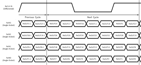
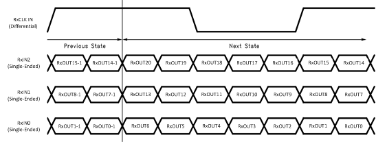
| ICCRW | Receiver Supply Current Worst Case | CL = 8 pF, Worst Case Pattern, DS90CR286A (Figure 1 Figure 2), TA=−10°C to +70°C | f = 33 MHz | 49 | 65 | mA | |
| f = 37.5 MHz | 53 | 70 | mA | ||||
| f = 66 MHz | 81 | 105 | mA | ||||
| ICCRW | Receiver Supply Current Worst Case | CL = 8 pF, Worst Case Pattern, DS90CR286A (Figure 1 Figure 2), TA=−40°C to +85°C | f = 40 MHz | 53 | 70 | mA | |
| f = 66 MHz | 81 | 105 | mA | ||||
| ICCRW | Receiver Supply Current Worst Case | CL = 8 pF, Worst Case Pattern, DS90CR216A (Figure 1 Figure 2), TA=−10°C to +70°C | f = 33 MHz | 49 | 55 | mA | |
| f = 37.5 MHz | 53 | 60 | mA | ||||
| f = 66 MHz | 78 | 90 | mA | ||||
| ICCRW | Receiver Supply Current Worst Case | CL = 8 pF, Worst Case Pattern, DS90CR216A (Figure 1 Figure 2), TA=−40°C to +85°C | f = 40 MHz | 53 | 60 | mA | |
| f = 66 MHz | 78 | 90 | mA | ||||
| ICCRZ | Receiver Supply Current Power Down | Power Down = Low Receiver Outputs Stay Low during Power Down Mode | 10 | 55 | μA | ||
(1) Typical values are given for VCC = 3.3 V and TA = 25ºC.
(2) Current into device pins is defined as positive. Current out of device pins is defined as negative. Voltages are referenced to ground unless otherwise specified (except VOD and ΔV OD).
6.6 Switching Characteristics: Receiver
over operating free-air temperature range (unless otherwise noted)(1)| PARAMETER | MIN | TYP | MAX | UNIT | ||
|---|---|---|---|---|---|---|
| CLHT | LVCMOS Low-to-High Transition Time (Figure 2) | 2 | 5 | ns | ||
| CHLT | LVCMOS High-to-Low Transition Time (Figure 2) | 1.8 | 5 | ns | ||
| RSPos0 | Receiver Input Strobe Position for Bit 0 (Figure 9, Figure 10) | f = 40 MHz | 1 | 1.4 | 2.15 | ns |
| RSPos1 | Receiver Input Strobe Position for Bit 1 | 4.5 | 5 | 5.8 | ns | |
| RSPos2 | Receiver Input Strobe Position for Bit 2 | 8.1 | 8.5 | 9.15 | ns | |
| RSPos3 | Receiver Input Strobe Position for Bit 3 | 11.6 | 11.9 | 12.6 | ns | |
| RSPos4 | Receiver Input Strobe Position for Bit 4 | 15.1 | 15.6 | 16.3 | ns | |
| RSPos5 | Receiver Input Strobe Position for Bit 5 | 18.8 | 19.2 | 19.9 | ns | |
| RSPos6 | Receiver Input Strobe Position for Bit 6 | 22.5 | 22.9 | 23.6 | ns | |
| RSPos0 | Receiver Input Strobe Position for Bit 0 (Figure 9, Figure 10) |
f = 66 MHz | 0.7 | 1.1 | 1.4 | ns |
| RSPos1 | Receiver Input Strobe Position for Bit 1 | 2.9 | 3.3 | 3.6 | ns | |
| RSPos2 | Receiver Input Strobe Position for Bit 2 | 5.1 | 5.5 | 5.8 | ns | |
| RSPos3 | Receiver Input Strobe Position for Bit 3 | 7.3 | 7.7 | 8 | ns | |
| RSPos4 | Receiver Input Strobe Position for Bit 4 | 9.5 | 9.9 | 10.2 | ns | |
| RSPos5 | Receiver Input Strobe Position for Bit 5 | 11.7 | 12.1 | 12.4 | ns | |
| RSPos6 | Receiver Input Strobe Position for Bit 6 | 13.9 | 14.3 | 14.6 | ns | |
| RSKM | RxIN Skew Margin(2) (Figure 11) | f = 40 MHz | 490 | ps | ||
| f = 66 MHz | 400 | ps | ||||
| RCOP | RxCLK OUT Period (Figure 3) | 15 | T | 50 | ns | |
| RCOH | RxCLK OUT High Time (Figure 3) | f = 40 MHz | 10 | 12.2 | ns | |
| RCOL | RxCLK OUT Low Time (Figure 3) | 10 | 11 | ns | ||
| RSRC | RxOUT Setup to RxCLK OUT (Figure 3) | 6.5 | 11.6 | ns | ||
| RHRC | RxOUT Hold to RxCLK OUT (Figure 3) | 6 | 11.6 | ns | ||
| RCOH | RxCLK OUT High Time (Figure 3) | f = 66 MHz | 5 | 7.6 | ns | |
| RCOL | RxCLK OUT Low Time (Figure 3) | 5 | 6.3 | ns | ||
| RSRC | RxOUT Setup to RxCLK OUT (Figure 3) | 4.5 | 7.3 | ns | ||
| RHRC | RxOUT Hold to RxCLK OUT (Figure 3) | 4 | 6.3 | ns | ||
| RCCD | RxCLK IN to RxCLK OUT Delay at 25°C, VCC = 3.3 V(3) (Figure 4) | 3.5 | 5 | 7.5 | ns | |
| RPLLS | Receiver Phase Lock Loop Set (Figure 5) | 10 | ms | |||
| RPDD | Receiver Power Down Delay (Figure 8) | 1 | μs | |||
(1) Typical Values are given for VCC = 3.3 V and TA = 25ºC
(2) Receiver Skew Margin is defined as the valid data sampling region at the receiver inputs. This margin takes into account the transmitter pulse positions (min and max) and the receiver input setup and hold time (internal data sampling window - RSPos). This margin allows for LVDS interconnect skew, inter-symbol interference (both dependent on type/length of cable), and clock jitter (less than 250 ps).
(3) Total latency for the channel link chipset is a function of clock period and gate delays through the transmitter (TCCD) and receiver (RCCD). The total latency for the DS90CR215/DS90CR285 transmitter and DS90CR216A/DS90CR286A receiver is: (T + TCCD) + (2*T + RCCD), where T = Clock period.
 Figure 1. “Worst Case” Test Pattern
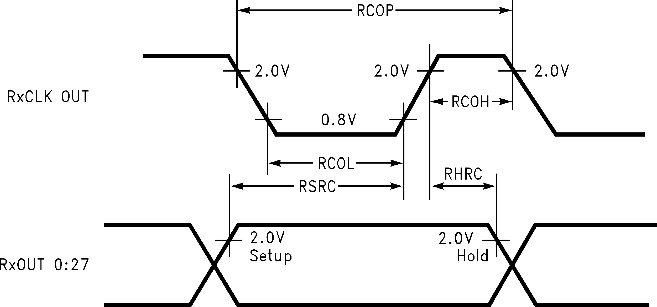 Figure 3. Setup/Hold and High/Low Times
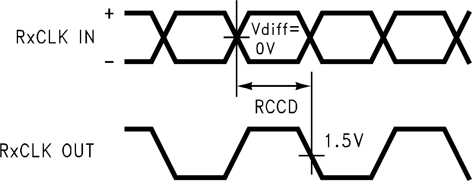 Figure 4. Clock In to Clock Out Delay
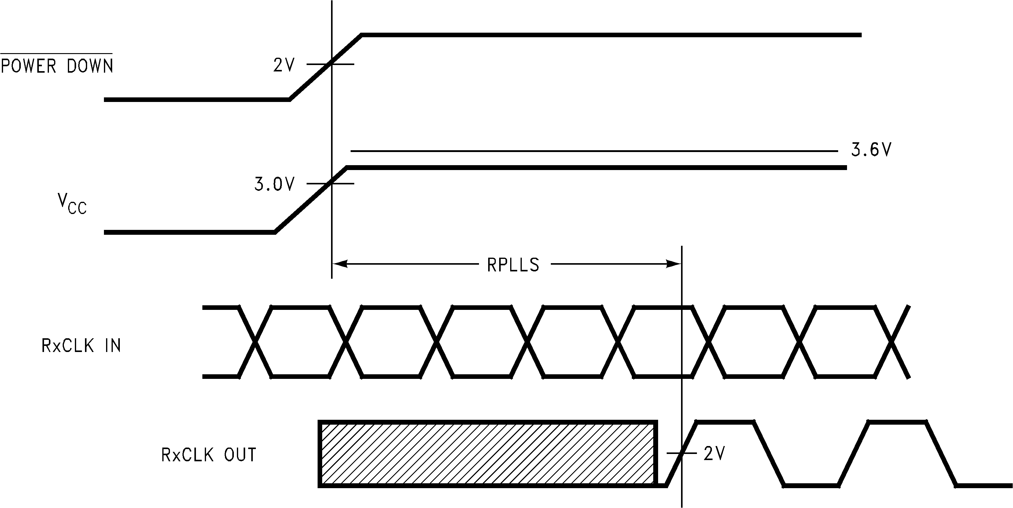 Figure 5. Phase Lock Loop Set Time
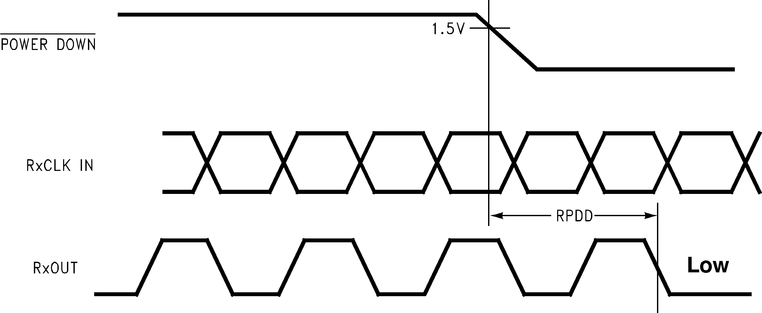 Figure 8. Power Down Delay
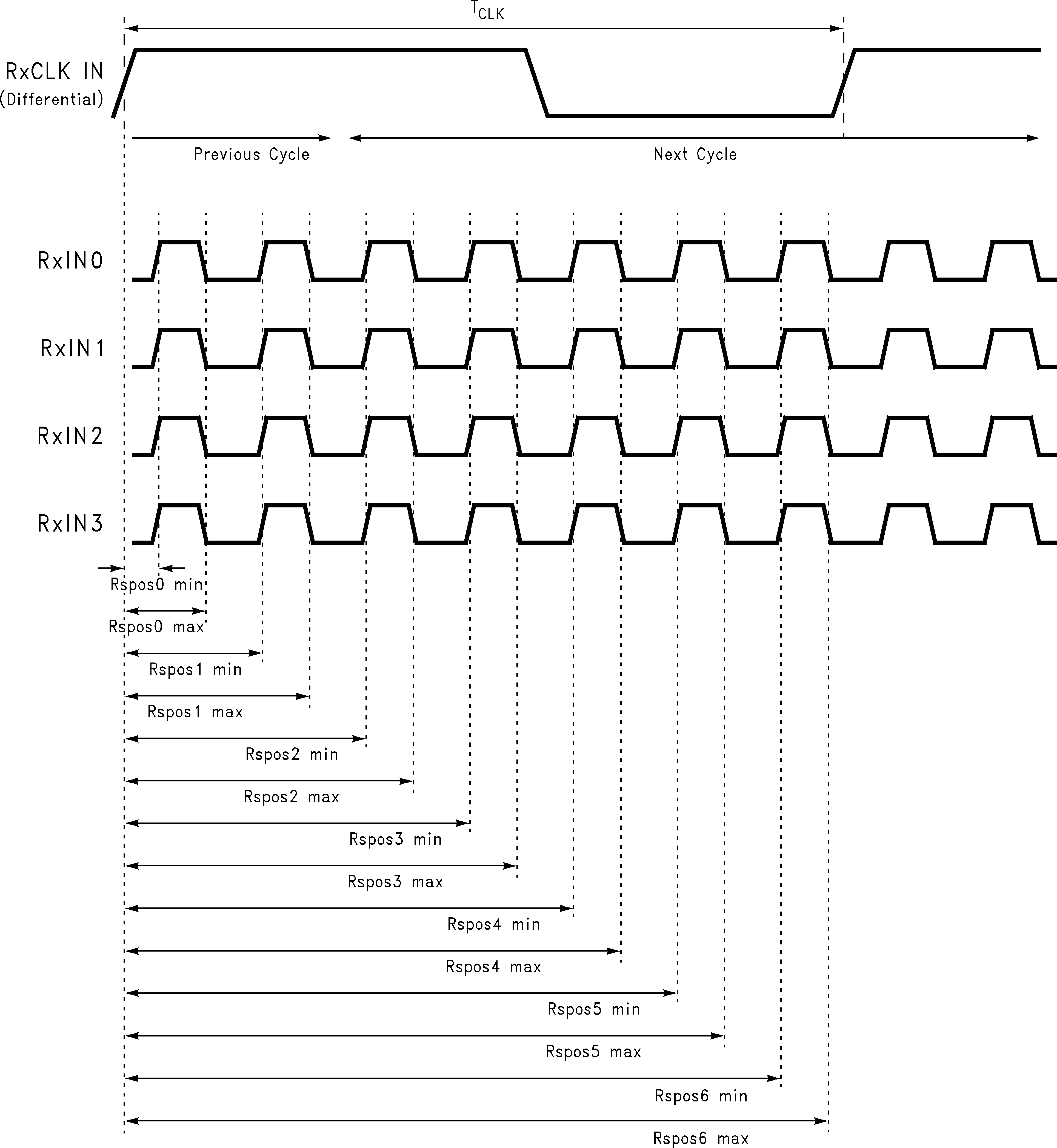 Figure 9. DS90CR286A LVDS Input Strobe Position
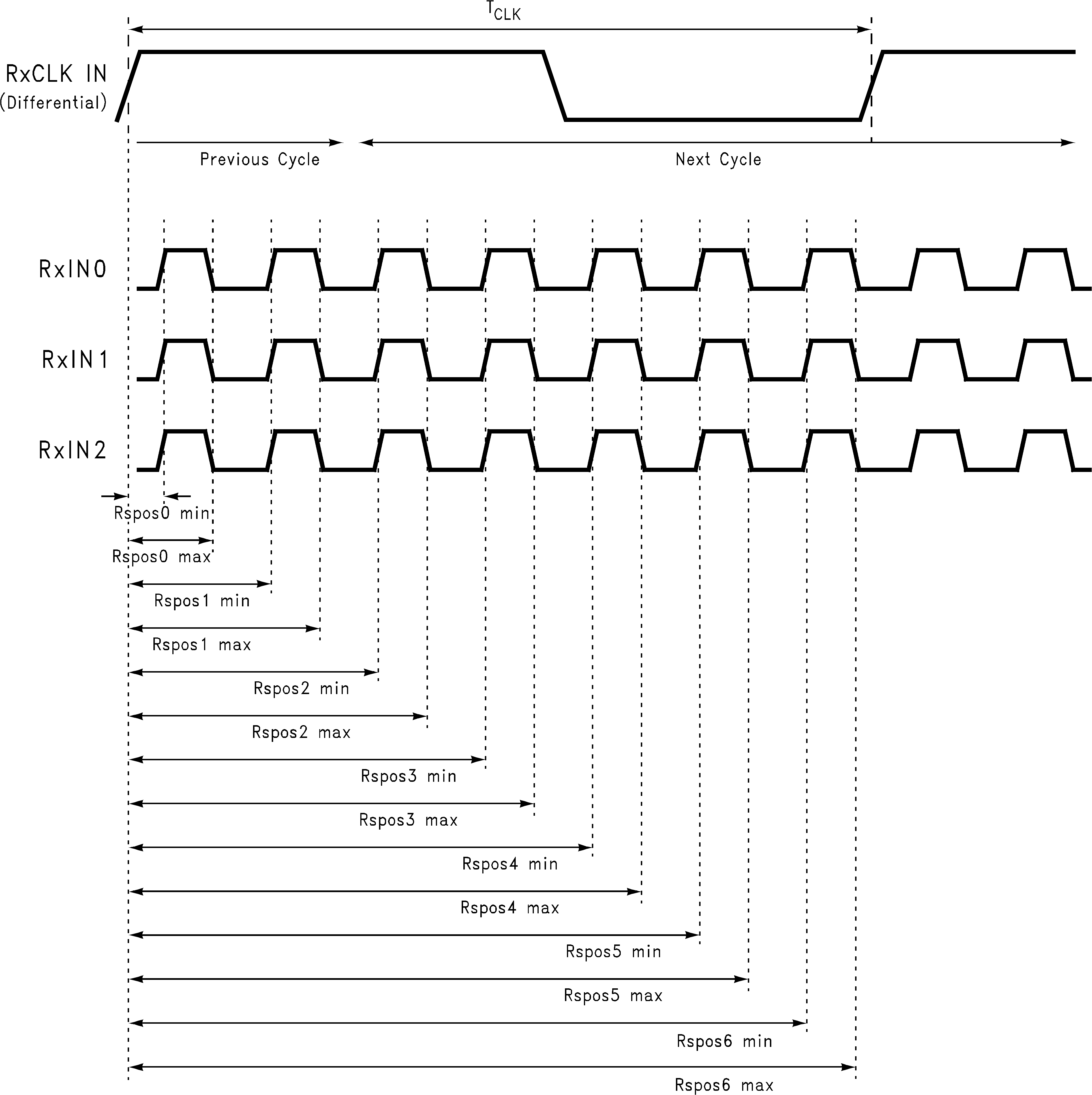 Figure 10. DS90CR216A LVDS Input Strobe Position

C—Setup and Hold Time (Internal data sampling window) defined by Rspos (receiver input strobe position) min and max
Tppos—Transmitter output pulse position (min and max)
Cable Skew—typically 10 ps–40 ps per foot, media dependent
RSKM = Cable Skew (type, length) + Source Clock Jitter (cycle to cycle)(1) + ISI (Inter-symbol interference)(2)
Tppos—Transmitter output pulse position (min and max)
Cable Skew—typically 10 ps–40 ps per foot, media dependent
RSKM = Cable Skew (type, length) + Source Clock Jitter (cycle to cycle)(1) + ISI (Inter-symbol interference)(2)
1. Cycle-to-cycle jitter depends on the Tx source. if a Channel Link I Source Transmitter is used, clock jitter is maintained to less than 250 ps at 66 MHz.
2. ISI is dependent on interconnect length; may be zero.
Figure 11. Receiver LVDS Input Skew Margin
6.7 Typical Characteristics
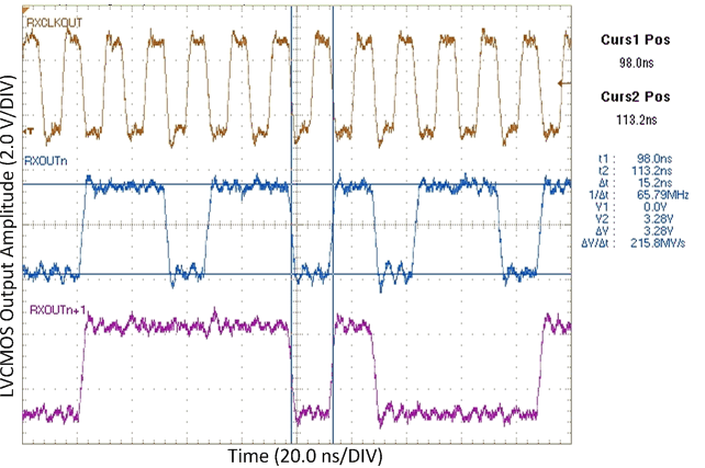 Figure 12. Parallel PRBS-7 on LVCMOS Outputs at 66 MHz
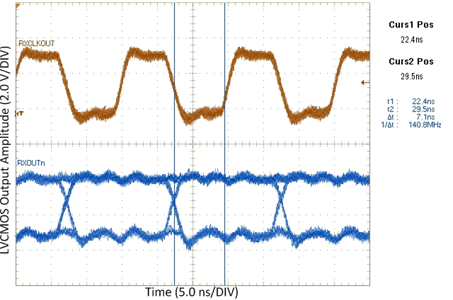 Figure 14. Typical RxOUT Setup Time at 66 MHz
 (RSRC = 7.1 ns)
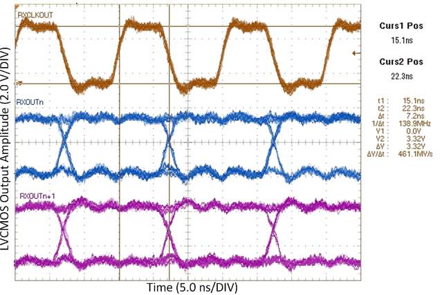 Figure 13. Typical RxOUT Strobe Position at 66 MHz
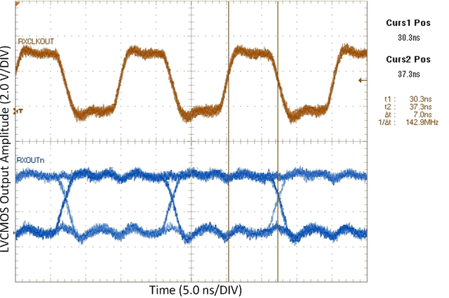 Figure 15. Typical RxOUT Hold Time at 66 MHz
 (RHRC = 7.0 ns)

