ZHCSET3A November 2015 – December 2015 DS90CR286AT-Q1
PRODUCTION DATA.
6 Specifications
6.1 Absolute Maximum Ratings
over operating free-air temperature range (unless otherwise noted) (1)| MIN | MAX | UNIT | |
|---|---|---|---|
| Supply Voltage (VCC) | −0.3 | 4 | V |
| LVCMOS Output Voltage | −0.3 | (VCC + 0.3) | V |
| LVDS Receiver Input Voltage | −0.3 | (VCC + 0.3) | V |
| Operating Junction Temperature | 150 | °C | |
| Lead Temperature (Soldering, 4 sec) | 260 | °C | |
| Storage temperature, Tstg | −65 | 150 | °C |
(1) Stresses beyond those listed under Absolute Maximum Ratings may cause permanent damage to the device. These are stress ratings only, which do not imply functional operation of the device at these or any other conditions beyond those indicated under Recommended Operating Conditions. Exposure to absolute-maximum-rated conditions for extended periods may affect device reliability.
6.2 ESD Ratings
| VALUE | UNIT | |||
|---|---|---|---|---|
| V(ESD) | Electrostatic discharge | Human-body model (HBM), per AEC Q100-002(1) | ±4000 | V |
| Charged-device model (CDM), per AEC Q100-011 | ±1000 | |||
(1) AEC Q100-002 indicates that HBM stressing shall be in accordance with the ANSI/ESDA/JEDEC JS-001 specification.
6.3 Recommended Operating Conditions
over operating free-air temperature range (unless otherwise noted)| MIN | NOM | MAX | UNIT | ||
|---|---|---|---|---|---|
| Supply Voltage (VCC) | 3.0 | 3.3 | 3.6 | V | |
| Operating Free Air Temperature (TA) | −40 | 25 | 105 | °C | |
| Receiver Input Range | 0 | 2.4 | V | ||
| Supply Noise Voltage (VNoise) | 100 | mVp-p | |||
6.4 Thermal Information
| THERMAL METRIC(1) | DS90CR286AT-Q1 | UNIT | |
|---|---|---|---|
| DGG (TSSOP) | |||
| 56 PINS | |||
| RθJA | Junction-to-ambient thermal resistance | 64.6 | °C/W |
| RθJC(top) | Junction-to-case (top) thermal resistance | 20.6 | |
| RθJB | Junction-to-board thermal resistance | 33.3 | |
| ψJT | Junction-to-top characterization parameter | 1.0 | |
| ψJB | Junction-to-board characterization parameter | 33.0 | |
(1) For more information about traditional and new thermal metrics, see the IC Package Thermal Metrics application report, SPRA953.
6.5 Electrical Characteristics(1)(2)
over operating free-air temperature range (unless otherwise noted)| PARAMETER | TEST CONDITIONS | MIN | TYP | MAX | UNIT | ||
|---|---|---|---|---|---|---|---|
| LVCMOS DC SPECIFICATIONS (For PWR DWN Pin) | |||||||
| VIH | High Level Input Voltage | 2.0 | VCC | V | |||
| VIL | Low Level Input Voltage | GND | 0.8 | V | |||
| VCL | Input Clamp Voltage | ICL = −18 mA | −0.79 | −1.5 | V | ||
| IIN | Input Current | VIN = 0.4 V, 2.5 V or VCC | +1.8 | +10 | μA | ||
| V IN = GND | −10 | 0 | μA | ||||
| LVCMOS DC SPECIFICATIONS | |||||||
| VOH | High Level Output Voltage | IOH = −0.4 mA | 2.7 | 3.3 | V | ||
| VOL | Low Level Output Voltage | IOL = 2 mA | 0.06 | 0.3 | V | ||
| IOS | Output Short Circuit Current | VOUT = 0 V | −60 | −120 | mA | ||
| LVDS RECEIVER DC SPECIFICATIONS | |||||||
| VTH | Differential Input High Threshold | VCM = 1.2 V | +100 | mV | |||
| VTL | Differential Input Low Threshold | VCM = 1.2 V | −100 | mV | |||
| IIN | Input Current | VIN = 2.4 V, VCC = 3.6 V | ±10 | μA | |||
| VIN = 0V , VCC = 3.6 V | ±10 | μA | |||||
| ICCRW | Receiver Supply Current Worst Case | CL = 8 pF, Worst Case Pattern, DS90CR286AT-Q1 (Figure 1 Figure 2), TA=−40°C to 105°C | f = 33 MHz | 49 | 65 | mA | |
| f = 40 MHz | 53 | 70 | mA | ||||
| f = 66 MHz | 81 | 105 | mA | ||||
| ICCRZ | Receiver Supply Current Power Down | PWR DWN = Low; Receiver Outputs Stay Low during Power Down Mode | 10 | 55 | μA | ||
(1) Typical values are given for VCC = 3.3 V and TA = 25ºC.
(2) Current into device pins is defined as positive. Current out of device pins is defined as negative. Voltages are referenced to ground unless otherwise specified (except VOD and ΔV OD).
6.6 Switching Characteristics
over operating free-air temperature range (unless otherwise noted)| PARAMETER | TEST CONDITIONS | MIN | TYP | MAX | UNIT | |
|---|---|---|---|---|---|---|
| CLHT | LVCMOS Low-to-High Transition Time (Figure 2) | 2 | 5 | ns | ||
| CHLT | LVCMOS High-to-Low Transition Time (Figure 2) | 1.8 | 5 | ns | ||
| RSPos0 | Receiver Input Strobe Position for Bit 0 (Figure 8) | f = 40 MHz, T = 25ºC | 1.01 | 1.4 | 2.45 | ns |
| RSPos1 | Receiver Input Strobe Position for Bit 1 | 4.52 | 5.0 | 5.99 | ns | |
| RSPos2 | Receiver Input Strobe Position for Bit 2 | 8.08 | 8.5 | 9.35 | ns | |
| RSPos3 | Receiver Input Strobe Position for Bit 3 | 11.59 | 11.9 | 12.89 | ns | |
| RSPos4 | Receiver Input Strobe Position for Bit 4 | 15.15 | 15.6 | 16.53 | ns | |
| RSPos5 | Receiver Input Strobe Position for Bit 5 | 18.86 | 19.2 | 20.20 | ns | |
| RSPos6 | Receiver Input Strobe Position for Bit 6 | 22.34 | 22.9 | 23.91 | ns | |
| RSPos0 | Receiver Input Strobe Position for Bit 0 (Figure 8) | f = 66 MHz, T = -40ºC | 0.58 | 1.1 | 1.55 | ns |
| RSPos1 | Receiver Input Strobe Position for Bit 1 | 2.77 | 3.3 | 3.80 | ns | |
| RSPos2 | Receiver Input Strobe Position for Bit 2 | 5.01 | 5.4 | 5.77 | ns | |
| RSPos3 | Receiver Input Strobe Position for Bit 3 | 7.11 | 7.5 | 7.88 | ns | |
| RSPos4 | Receiver Input Strobe Position for Bit 4 | 9.24 | 9.7 | 10.12 | ns | |
| RSPos5 | Receiver Input Strobe Position for Bit 5 | 11.44 | 11.9 | 12.32 | ns | |
| RSPos6 | Receiver Input Strobe Position for Bit 6 | 13.62 | 14.1 | 14.50 | ns | |
| RSPos0 | Receiver Input Strobe Position for Bit 0 (Figure 8) | f = 66 MHz, T = 25ºC | 0.68 | 1.2 | 1.64 | ns |
| RSPos1 | Receiver Input Strobe Position for Bit 1 | 2.88 | 3.4 | 3.88 | ns | |
| RSPos2 | Receiver Input Strobe Position for Bit 2 | 5.08 | 5.5 | 5.87 | ns | |
| RSPos3 | Receiver Input Strobe Position for Bit 3 | 7.20 | 7.6 | 7.98 | ns | |
| RSPos4 | Receiver Input Strobe Position for Bit 4 | 9.30 | 9.7 | 10.24 | ns | |
| RSPos5 | Receiver Input Strobe Position for Bit 5 | 11.50 | 12.0 | 12.40 | ns | |
| RSPos6 | Receiver Input Strobe Position for Bit 6 | 13.70 | 14.2 | 14.57 | ns | |
| RSPos0 | Receiver Input Strobe Position for Bit 0 (Figure 8) | f = 66 MHz, T = 105ºC | 0.84 | 1.3 | 1.74 | ns |
| RSPos1 | Receiver Input Strobe Position for Bit 1 | 3.00 | 3.6 | 4.05 | ns | |
| RSPos2 | Receiver Input Strobe Position for Bit 2 | 5.14 | 5.6 | 6.02 | ns | |
| RSPos3 | Receiver Input Strobe Position for Bit 3 | 7.30 | 7.8 | 8.14 | ns | |
| RSPos4 | Receiver Input Strobe Position for Bit 4 | 9.42 | 9.9 | 10.40 | ns | |
| RSPos5 | Receiver Input Strobe Position for Bit 5 | 11.59 | 12.1 | 12.57 | ns | |
| RSPos6 | Receiver Input Strobe Position for Bit 6 | 13.83 | 14.3 | 14.73 | ns | |
| RCOP | RxCLK OUT Period (Figure 3) | 15 | 50 | ns | ||
| RCOH | RxCLK OUT High Time (Figure 3) | f = 40 MHz | 10.0 | 12.2 | ns | |
| RCOL | RxCLK OUT Low Time (Figure 3) | 10.0 | 11.0 | ns | ||
| RSRC | RxOUT Setup to RxCLK OUT (Figure 3) | 6.5 | 11.6 | ns | ||
| RHRC | RxOUT Hold to RxCLK OUT (Figure 3) | 6.0 | 11.6 | ns | ||
| RCOH | RxCLK OUT High Time (Figure 3) | f = 66 MHz | 5.0 | 7.6 | ns | |
| RCOL | RxCLK OUT Low Time (Figure 3) | 5.0 | 6.3 | ns | ||
| RSRC | RxOUT Setup to RxCLK OUT (Figure 3) | 4.5 | 7.3 | ns | ||
| RHRC | RxOUT Hold to RxCLK OUT (Figure 3) | 4.0 | 6.3 | ns | ||
| RCCD | RxCLK IN to RxCLK OUT Delay at 25°C, VCC = 3.3V(1) (Figure 4) | 3.5 | 5.0 | 7.5 | ns | |
| RPLLS | Receiver Phase Lock Loop Set (Figure 5) | 10 | ms | |||
| RPDD | Receiver Power Down Delay (Figure 7) | 1 | μs | |||
(1) Total latency for the channel link chipset is a function of clock period and gate delays through the transmitter (TCCD) and receiver (RCCD). The total latency for the DS90CR285 transmitter and DS90CR286AT-Q1 receiver is: (T + TCCD) + (2*T + RCCD), where T = Clock period. If another transmitter is used, the alternative transmitter's TCCD must be used to calculate total latency.
 Figure 1. "Worst Case" Test Pattern
 Figure 2. LVCMOS Output Load and Transition Times
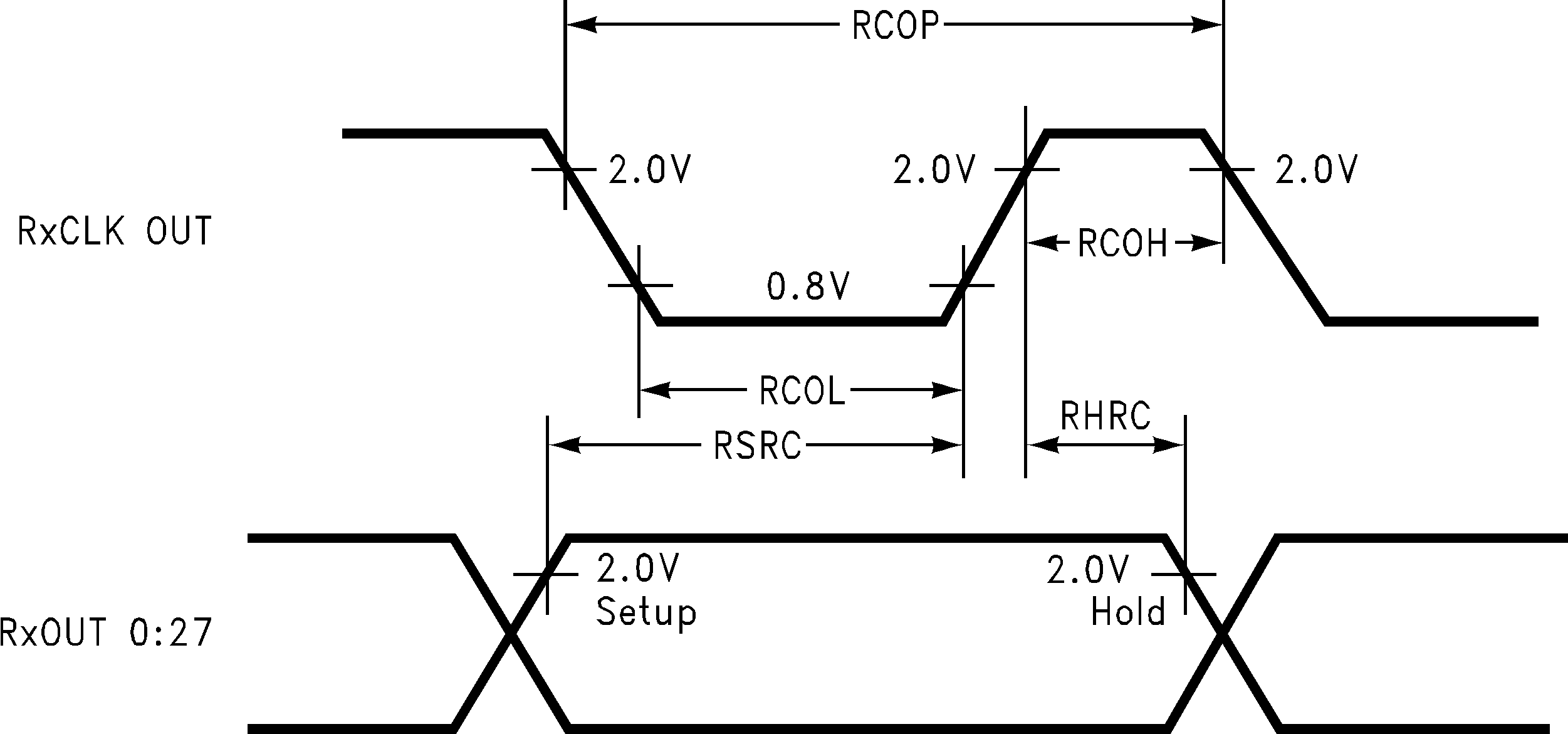 Figure 3. Setup/Hold and High/Low Times
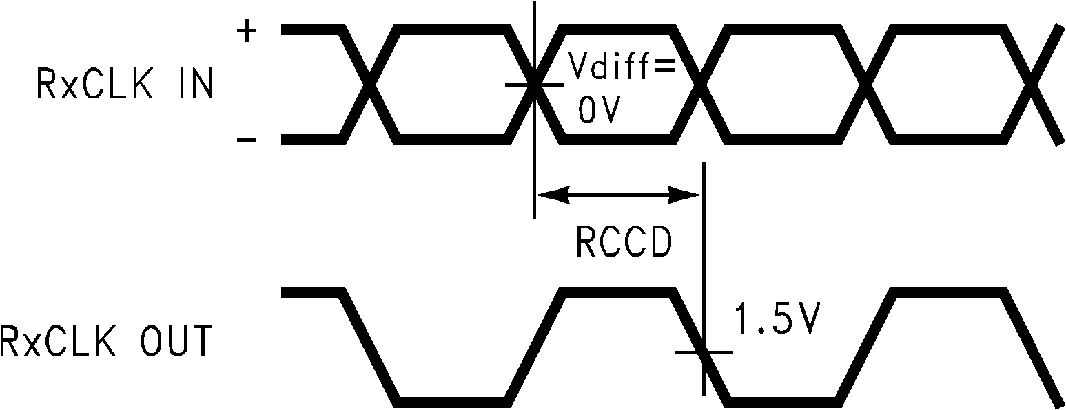 Figure 4. Clock In to Clock Out Delay
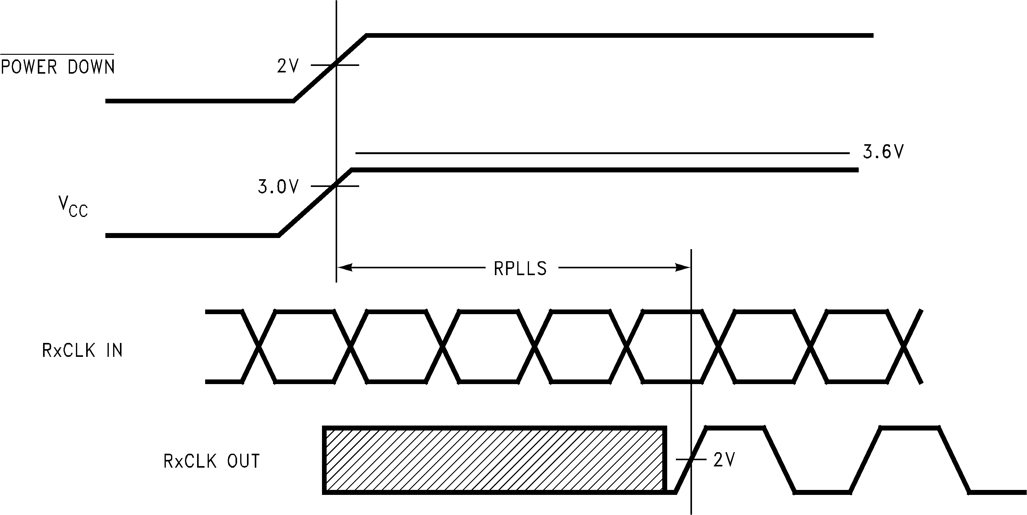 Figure 5. Phase Lock Loop Set Time
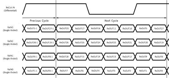 Figure 6. Mapping of 28 LVCMOS Parallel Data to 4D + C LVDS Serialized Data
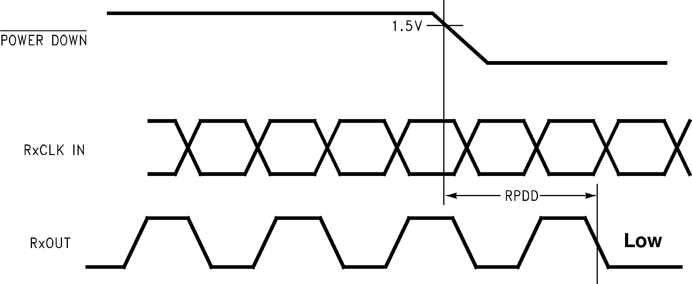 Figure 7. Power Down Delay
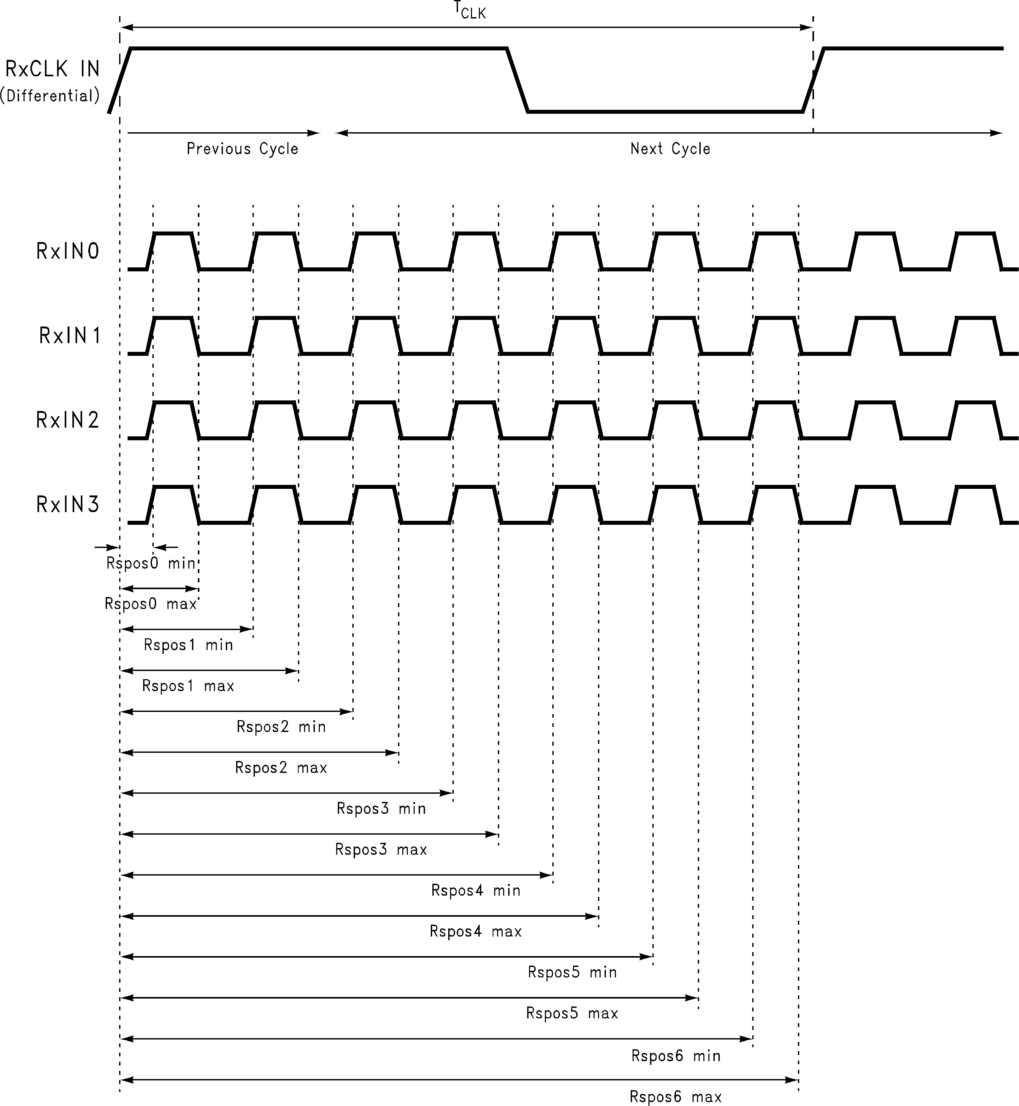 Figure 8. LVDS Input Strobe Position
6.7 Typical Characteristics
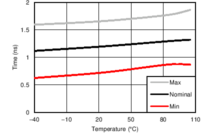 Figure 9. Rx Strobe Position 0 versus Temperature
Operating Frequency: 66 MHz
 Figure 11. Rx Strobe Position 2 versus Temperature
Operating Frequency: 66 MHz
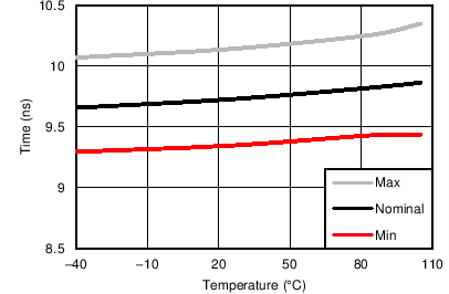 Figure 13. Rx Strobe Position 4 versus Temperature
Operating Frequency: 66 MHz
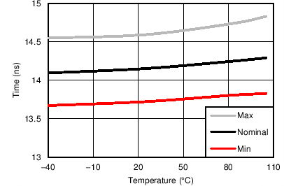 Figure 15. Rx Strobe Position 6 versus Temperature
Operating Frequency: 66 MHz
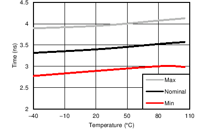 Figure 10. Rx Strobe Position 1 versus Temperature
Operating Frequency: 66 MHz
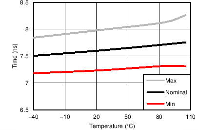 Figure 12. Rx Strobe Position 3 versus Temperature
Operating Frequency: 66 MHz
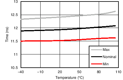 Figure 14. Rx Strobe Position 5 versus Temperature
Operating Frequency: 66 MHz
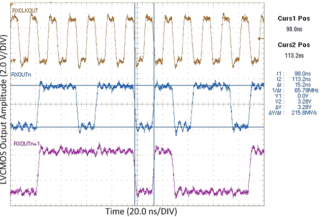 Figure 16. Parallel PRBS-7 on LVCMOS Outputs at 66 MHz
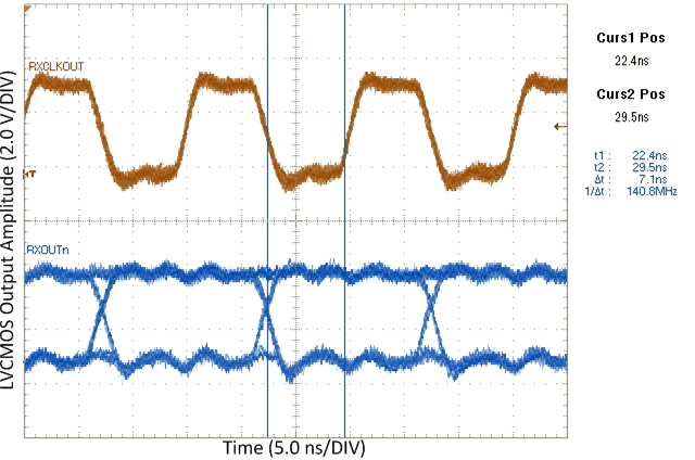 Figure 18. Typical RxOUT Setup Time at 66 MHz
 (RSRC = 7.1 ns)
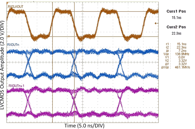 Figure 17. Typical RxOUT Timing Diagram at 66 MHz
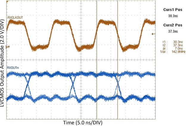 Figure 19. Typical RxOUT Hold Time at 66 MHz
 (RHRC = 7.0 ns)