ZHCSET3A November 2015 – December 2015 DS90CR286AT-Q1
PRODUCTION DATA.
8 Application and Implementation
NOTE
Information in the following applications sections is not part of the TI component specification, and TI does not warrant its accuracy or completeness. TI’s customers are responsible for determining suitability of components for their purposes. Customers should validate and test their design implementation to confirm system functionality.
8.1 Application Information
The DS90CR286AT-Q1 is designed for a wide variety of data transmission applications. The use of serialized LVDS data lines in these applications allows for efficient signal transmission over a narrow bus width, thereby reducing cost, power, and space. The DS90CR286AT-Q1 is designed for PCB board chip-to-chip OpenLDI-to-RGB (LVDS-to-parallel) bridge conversion. LVDS data transmission over cable interconnect is not recommended for this device. Users designing a sub-system with a compatible OpenLDI transmitter and DS90CR286AT-Q1 receiver must ensure an acceptable skew margin budget (RSKM).
8.2 Typical Application
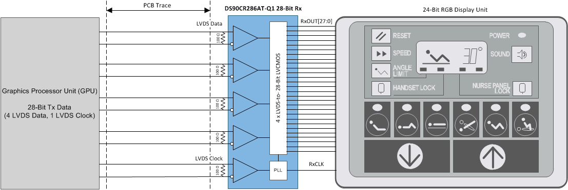 Figure 22. Typical DS90CR286AT-Q1 Application Block Diagram
8.2.1 Design Requirements
For this design example, ensure that the following requirements are observed.
Table 1. DS90CR286AT-Q1 Design Parameters
| DESIGN PARAMETER | DESIGN REQUIREMENTS |
|---|---|
| Operating Frequency | LVDS clock must be within 20-66 MHz. |
| Bit Resolution | No higher than 24 bpp. The maximum supported resolution is 8-bit RGB. |
| Bit Data Mapping | Determine the appropriate mapping required by the panel display following the DS90CR286AT-Q1 outputs. |
| RSKM (Receiver Skew Margin) | Ensure that there is acceptable margin between Tx pulse position and Rx strobe position. |
| Input Termination for RxIN± | 100 Ω ± 10% resistor across each LVDS differential pair. Place as close as possible to IC input pins. |
| RxIN± Board Trace Impedance | Design differential trace impedance with 100 Ω ± 5%. |
| LVCMOS Outputs | If unused, leave pins floating. Series resistance on each LVCMOS output optional to reduce reflections from long board traces. If used, 33 Ω series resistance is typical. |
| DC Power Supply Coupling Capacitors | Use a 0.1 µF capacitor to minimize power supply noise. Place as close as possible to Vcc pins. |
8.2.2 Detailed Design Procedure
To begin the design process with the DS90CR286AT-Q1, determine the following:
- Operating Frequency
- Bit Resolution of the Panel
- Bit Mapping from Receiver to Endpoint Panel Display
- RSKM Interoperability with Transmitter Pulse Position Margin
8.2.2.1 Bit Resolution and Operating Frequency Compatibility
The bit resolution of the endpoint panel display reveals whether there are enough bits available in the DS90CR286AT-Q1 to output the required data per pixel. The DS90CR286AT-Q1 has 28 parallel LVCMOS outputs and can therefore provide a bit resolution up to 24 bpp (bits per pixel). In each clock cycle, the remaining bits are the three control signals (HSync, VSync, DE) and one spare bit.
The number of pixels per frame and the refresh rate of the endpoint panel display indicate the required operating frequency of the receiver clock. To determine the required clock frequency, refer to the following formula:
where
- H_Active = Active Display Horizontal Lines
- H_Blank = Blanking Period Horizontal Lines
- V_Active = Active Display Vertical Lines
- V_Blank = Blanking Period Vertical Lines
- f_Vertical = Refresh Rate (in Hz)
- f_Clk = Operating Frequency of LVDS clock
In each frame, there is a blanking period associated with horizontal rows and vertical columns that are not actively displayed on the panel. These blanking period pixels must be included to determine the required clock frequency. Consider the following example to determine the required LVDS clock frequency:
- H_Active = 640
- H_Blank = 40
- V_Active = 480
- V_Blank = 41
- f_Vertical = 59.95 Hz
Thus, the required operating frequency is determined below:
Since the operating frequency for the PLL in the DS90CR286AT-Q1 ranges from 20-66 MHz, the DS90CR286AT-Q1 can support a panel display with the aforementioned requirements.
If the specific blanking interval is unknown, the number of pixels in the blanking interval can be approximated to 20% of the active pixels. The following formula can be used as a conservative approximation for the operating LVDS clock frequency:
Using this approximation, the operating frequency for the example in this section is estimated below:
8.2.2.2 Data Mapping between Receiver and Endpoint Panel Display
Ensure that the LVCMOS outputs are mapped to align with the endpoint display RGB mapping requirements following the deserializer. Two popular mapping topologies for 8-bit RGB data are shown below:
- LSBs are mapped to RxIN3±.
- MSBs are mapped to RxIN3±.
The following tables depict how these two popular topologies can be mapped to the DS90CR286AT-Q1 outputs.
Table 2. 8-Bit Color Mapping with LSBs on RxIN3±
| LVDS INPUT CHANNEL | LVDS BIT STREAM POSITION | LVCMOS OUTPUT CHANNEL | COLOR MAPPING | COMMENTS |
|---|---|---|---|---|
| RxIN0 | TxIN0 | RxOUT0 | R2 | |
| TxIN1 | RxOUT1 | R3 | ||
| TxIN2 | RxOUT2 | R4 | ||
| TxIN3 | RxOUT3 | R5 | ||
| TxIN4 | RxOUT4 | R6 | ||
| TxIN6 | RxOUT6 | R7 | MSB | |
| RxIN1 | TxIN7 | RxOUT7 | G2 | |
| TxIN8 | RxOUT8 | G3 | ||
| TxIN9 | RxOUT9 | G4 | ||
| TxIN12 | RxOUT12 | G5 | ||
| TxIN13 | RxOUT13 | G6 | ||
| TxIN14 | RxOUT14 | G7 | MSB | |
| TxIN15 | RxOUT15 | B2 | ||
| TxIN18 | RxOUT18 | B3 | ||
| RxIN2 | TxIN19 | RxOUT19 | B4 | |
| TxIN20 | RxOUT20 | B5 | ||
| TxIN21 | RxOUT21 | B6 | ||
| TxIN22 | RxOUT22 | B7 | MSB | |
| TxIN24 | RxOUT24 | HSYNC | Horizontal Sync | |
| TxIN25 | RxOUT25 | VSYNC | Vertical Sync | |
| TxIN26 | RxOUT26 | DE | Data Enable | |
| RxIN3 | TxIN27 | RxOUT27 | R0 | LSB |
| TxIN5 | RxOUT5 | R1 | ||
| TxIN10 | RxOUT10 | G0 | LSB | |
| TxIN11 | RxOUT11 | G1 | ||
| TxIN16 | RxOUT16 | B0 | LSB | |
| TxIN17 | RxOUT17 | B1 | ||
| TxIN23 | RxOUT23 | GP | General Purpose |
Table 3. 8-Bit Color Mapping with MSBs on RxIN3±
| LVDS INPUT CHANNEL | LVDS BIT STREAM POSITION | LVCMOS OUTPUT CHANNEL | COLOR MAPPING | COMMENTS |
|---|---|---|---|---|
| RxIN0 | TxIN0 | RxOUT0 | R0 | LSB |
| TxIN1 | RxOUT1 | R1 | ||
| TxIN2 | RxOUT2 | R2 | ||
| TxIN3 | RxOUT3 | R3 | ||
| TxIN4 | RxOUT4 | R4 | ||
| TxIN6 | RxOUT6 | R5 | ||
| RxIN1 | TxIN7 | RxOUT7 | G0 | LSB |
| TxIN8 | RxOUT8 | G1 | ||
| TxIN9 | RxOUT9 | G2 | ||
| TxIN12 | RxOUT12 | G3 | ||
| TxIN13 | RxOUT13 | G4 | ||
| TxIN14 | RxOUT14 | G5 | ||
| TxIN15 | RxOUT15 | B0 | LSB | |
| TxIN18 | RxOUT18 | B1 | ||
| RxIN2 | TxIN19 | RxOUT19 | B2 | |
| TxIN20 | RxOUT20 | B3 | ||
| TxIN21 | RxOUT21 | B4 | ||
| TxIN22 | RxOUT22 | B5 | ||
| TxIN24 | RxOUT24 | HSYNC | Horizontal Sync | |
| TxIN25 | RxOUT25 | VSYNC | Vertical Sync | |
| TxIN26 | RxOUT26 | DE | Data Enable | |
| RxIN3 | TxIN27 | RxOUT27 | R6 | |
| TxIN5 | RxOUT5 | R7 | MSB | |
| TxIN10 | RxOUT10 | G6 | ||
| TxIN11 | RxOUT11 | G7 | MSB | |
| TxIN16 | RxOUT16 | B6 | ||
| TxIN17 | RxOUT17 | B7 | MSB | |
| TxIN23 | RxOUT23 | GP | General Purpose |
In situations where the DS90CR286AT-Q1 must support 18 bpp, Table 2 is commonly used. With this mapping, MSBs of RGB data are retained on RXIN0±, RXIN1±, and RXIN2± while the two LSBs for the original 8-bit RGB resolution are ignored from RxIN3±.
8.2.2.3 RSKM Interoperability
One of the most important factors when designing the receiver into a system application is assessing how much RSKM (Receiver Skew Margin) is available. In each LVDS clock cycle, the LVDS data stream carries seven serialized data bits. Ideally, the Transmit Pulse Position for each bit will occur every (n x T)/7 seconds, where n = Bit Position and T = LVDS Clock Period. Likewise, ideally the Receive Strobe Position for each bit will occur every ((n + 0.5) x T)/7 seconds. However, due to the effects of clock jitter and ISI, both LVDS transmitter and receiver in real systems will have a minimum and maximum pulse and strobe position, respectively, for each bit position. This concept is illustrated in Figure 23:
 Figure 23. RSKM Measurement Example
All left and right margins for Bits 0-6 must be considered in order to determine the absolute minimum for the whole LVDS bit stream. This absolute minimum corresponds to the RSKM.
To improve RSKM performance between LVDS transmitter and receiver, designers may either advance or delay the LVDS clock compared to the LVDS data. Moving the LVDS clock compared to the LVDS data can improve the Rx strobe position compared to the Tx pulse position of the transmitter.
If there is less left bit margin than right bit margin, the LVDS clock can be delayed so that the Rx strobe position for incoming data appears to be delayed. If there is less right bit margin than left bit margin, all the LVDS data pairs can be delayed uniformly so that the LVDS clock and Rx strobe position for incoming data appear to advance. To delay an LVDS data or clock pair, designers can either add more PCB trace length or install a capacitor between the LVDS transmitter and receiver. It is important to note that when using these techniques, all serialized bit positions are shifted right or left uniformly.
When designing the DS90CR286AT-Q1 receiver with a third-party OpenLDI transmitter, users must calculate the skew margin budget (RSKM) based on the Tx pulse position and the Rx strobe position to ensure error-free transmission. For more information about calculating RSKM, refer to Application Note SNLA249.
8.2.3 Application Curves
The following application curves are examples taken with a DS90C385 serializer interfacing to a DS90CR286AT-Q1 deserializer in nominal temperature (25ºC) at an operating frequency of 66 MHz.
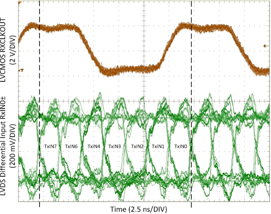 Figure 24. LVDS RxIN0± aligned with LVCMOS RxCLKOUT
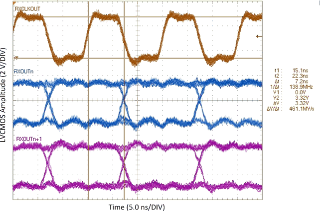 Figure 26. RxOUT and RxCLKOUT Timing Diagram
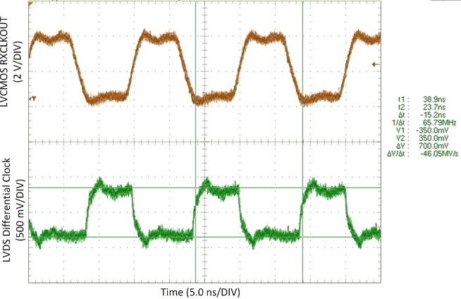 Figure 25. LVDS CLKIN aligned with LVCMOS RxCLKOUT
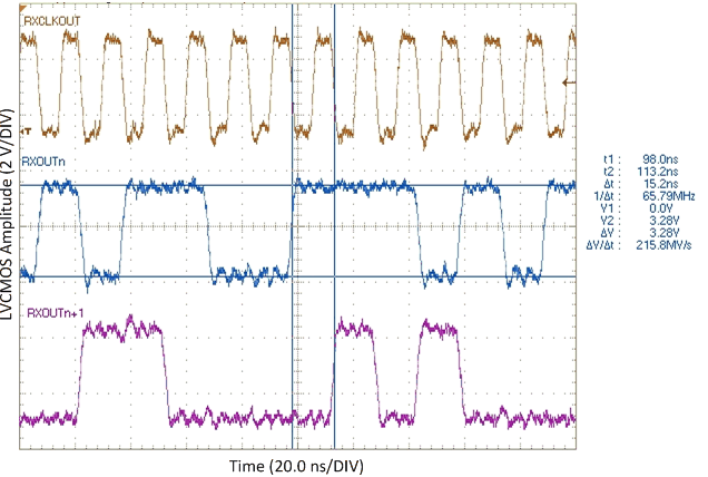 Figure 27. PRBS-7 Output on RxOUT Channels