SNLS044D May 2000 – July 2016 DS90LV047A
PRODUCTION DATA.
- 1 Features
- 2 Applications
- 3 Description
- 4 Revision History
- 5 Pin Configuration and Functions
- 6 Specifications
- 7 Parameter Measurement Information
- 8 Detailed Description
- 9 Application and Implementation
- 10Power Supply Recommendations
- 11Layout
- 12Device and Documentation Support
- 13Mechanical, Packaging, and Orderable Information
9 Application and Implementation
NOTE
Information in the following applications sections is not part of the TI component specification, and TI does not warrant its accuracy or completeness. TI’s customers are responsible for determining suitability of components for their purposes. Customers should validate and test their design implementation to confirm system functionality.
9.1 Application Information
The DS90LV047A has a flow-through pinout that allows for easy PCB layout. The LVDS signals on one side of the device easily allows for matching electrical lengths of the differential pair trace lines between the driver and the receiver as well as allowing the trace lines to be close together to couple noise as common-mode. Noise isolation is achieved with the LVDS signals on one side of the device and the TTL signals on the other side.
9.2 Typical Application
 Figure 23. Point-to-Point Application
9.2.1 Design Requirements
When using LVDS devices, it is important to remember to specify controlled impedance PCB traces, cable assemblies, and connectors. All components of the transmission media should have a matched differential impedance of about 100 Ω. They should not introduce major impedance discontinuities.
Balanced cables (for example, twisted pair) are usually better than unbalanced cables (ribbon cable) for noise reduction and signal quality. Balanced cables tend to generate less EMI due to field canceling effects and also tend to pick up electromagnetic radiation as common-mode (not differential mode) noise which is rejected by the LVDS receiver.
For cable distances < 0.5 M, most cables can be made to work effectively. For distances 0.5 M ≤ d ≤ 10 M, CAT5 (Category 5) twisted pair cable works well, is readily available and relatively inexpensive.
9.2.2 Detailed Design Procedure
9.2.2.1 Probing LVDS Transmission Lines
Always use high impedance (> 100 kΩ), low capacitance (< 2 pF) scope probes with a wide bandwidth (1 GHz) scope. Improper probing gives deceiving results.
9.2.2.2 Data Rate vs Cable Length Graph Test Procedure
A pseudo-random bit sequence (PRBS) of 29−1 bits was programmed into a function generator (Tektronix HFS9009) and connected to the driver inputs through 50-Ω cables and SMB connectors. An oscilloscope (Tektronix 11801B) was used to probe the resulting eye pattern, measured differentially at the input to the receiver. A 100-Ω resistor was used to terminate the pair at the far end of the cable. The measurements were taken at the far end of the cable, at the input of the receiver, and used for the jitter analysis for this graph (Figure 16). The frequency of the input signal was increased until the measured jitter (ttcs) equaled 20% with respect to the unit interval (ttui) for the particular cable length under test. Twenty percent jitter is a reasonable place to start with many system designs. The data used was NRZ. Jitter was measured at the 0-V differential voltage of the differential eye pattern. The DS90LV047A and DS90LV048A can be evaluated using the new DS90LV047-048AEVM.
Figure 24 shows very good typical performance that can be used as a design guideline for data rate vs cable length. Increasing the jitter percentage increases the curve respectively, allowing the device to transmit faster over longer cable lengths. This relaxes the jitter tolerance of the system allowing more jitter into the system, which could reduce the reliability and efficiency of the system. Alternatively, decreasing the jitter percentage has the opposite effect on the system. The area under the curve is considered the safe operating area based on the above signal quality criteria. For more information on eye pattern testing, please see AN-808 Long Transmission Lines and Data Signal Quality (SNLA028).
9.2.3 Application Curve
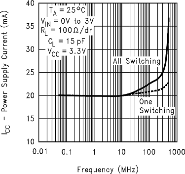
 Figure 24. Power Supply Current vs Frequency