SNLS044D May   2000  – July 2016 DS90LV047A

PRODUCTION DATA.  

  1. Features
  2. Applications
  3. Description
  4. Revision History
  5. Pin Configuration and Functions
  6. Specifications
    1. 6.1 Absolute Maximum Ratings
    2. 6.2 ESD Ratings
    3. 6.3 Recommended Operating Conditions
    4. 6.4 Thermal Information
    5. 6.5 Electrical Characteristics
    6. 6.6 Switching Characteristics
    7. 6.7 Typical Characteristics
  7. Parameter Measurement Information
  8. Detailed Description
    1. 8.1 Overview
    2. 8.2 Functional Block Diagram
    3. 8.3 Feature Description
      1. 8.3.1 LVDS Fail-Safe
    4. 8.4 Device Functional Modes
  9. Application and Implementation
    1. 9.1 Application Information
    2. 9.2 Typical Application
      1. 9.2.1 Design Requirements
      2. 9.2.2 Detailed Design Procedure
        1. 9.2.2.1 Probing LVDS Transmission Lines
        2. 9.2.2.2 Data Rate vs Cable Length Graph Test Procedure
      3. 9.2.3 Application Curve
  10. 10Power Supply Recommendations
  11. 11Layout
    1. 11.1 Layout Guidelines
      1. 11.1.1 Power Decoupling Recommendations
      2. 11.1.2 Differential Traces
      3. 11.1.3 Termination
    2. 11.2 Layout Example
  12. 12Device and Documentation Support
    1. 12.1 Documentation Support
      1. 12.1.1 Related Documentation
    2. 12.2 Receiving Notification of Documentation Updates
    3. 12.3 Community Resources
    4. 12.4 Trademarks
    5. 12.5 Electrostatic Discharge Caution
    6. 12.6 Glossary
  13. 13Mechanical, Packaging, and Orderable Information

封装选项

机械数据 (封装 | 引脚)
散热焊盘机械数据 (封装 | 引脚)
订购信息

7 Parameter Measurement Information

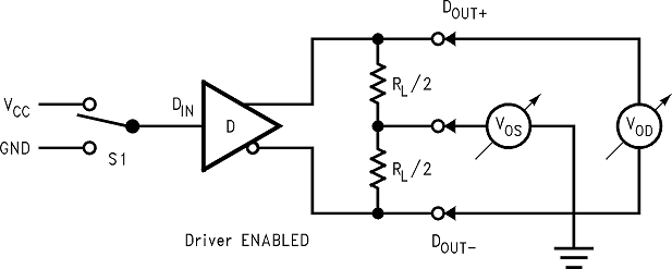
DS90LV047A 10088703.png Figure 17. Driver VOD and VOS Test Circuit
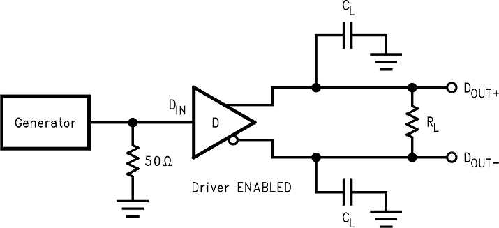
DS90LV047A 10088704.png Figure 18. Driver Propagation Delay and Transition Time Test Circuit
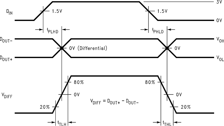
DS90LV047A 10088705.png Figure 19. Driver Propagation Delay and Transition Time Waveforms
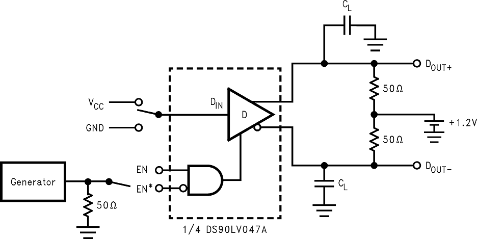
DS90LV047A 10088706.png Figure 20. Driver TRI-STATE Delay Test Circuit
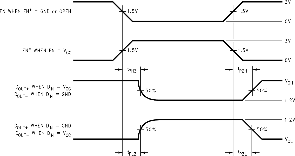
DS90LV047A 10088707.png Figure 21. Driver TRI-STATE Delay Waveform