ZHCSMR4A november 2020 – november 2020 DS90UB662-Q1
PRODUCTION DATA
- 1
- 1 特性
- 2 应用
- 3 说明
- 4 Revision History
- 5 Pin Configuration and Functions
- 6 Specifications
-
7 Detailed Description
- 7.1 Overview
- 7.2 Functional Block Diagram
- 7.3 Feature Description
- 7.4
Device Functional Modes
- 7.4.1 CSI-2 Mode
- 7.4.2 RAW Mode
- 7.4.3 MODE Pin
- 7.4.4 REFCLK
- 7.4.5 Receiver Port Control
- 7.4.6 Input Jitter Tolerance
- 7.4.7 Adaptive Equalizer
- 7.4.8 Channel Monitor Loop-Through Output Driver
- 7.4.9 RX Port Status
- 7.4.10 Sensor Status
- 7.4.11 GPIO Support
- 7.4.12 RAW Mode LV / FV Controls
- 7.4.13 CSI-2 Protocol Layer
- 7.4.14 CSI-2 Short Packet
- 7.4.15 CSI-2 Long Packet
- 7.4.16 CSI-2 Data Identifier
- 7.4.17 Virtual Channel and Context
- 7.4.18 CSI-2 Mode Virtual Channel Mapping
- 7.4.19 CSI-2 Transmitter Frequency
- 7.4.20 CSI-2 Output Bandwidth
- 7.4.21 CSI-2 Transmitter Status
- 7.4.22 Video Buffers
- 7.4.23 CSI-2 Line Count and Line Length
- 7.4.24 FrameSync Operation
- 7.4.25
CSI-2 Forwarding
- 7.4.25.1 Best-Effort Round Robin CSI-2 Forwarding
- 7.4.25.2 Synchronized CSI-2 Forwarding
- 7.4.25.3 Basic Synchronized CSI-2 Forwarding
- 7.4.25.4 Line-Interleaved CSI-2 Forwarding
- 7.4.25.5 Line-Concatenated CSI-2 Forwarding
- 7.4.25.6 CSI-2 Transmitter Output Control
- 7.4.25.7 Enabling and Disabling CSI-2 Transmitters
- 7.5
Programming
- 7.5.1 Serial Control Bus
- 7.5.2 Second I2C Port
- 7.5.3 I2C Slave Operation
- 7.5.4 Remote Slave Operation
- 7.5.5 Remote Slave Addressing
- 7.5.6 Broadcast Write to Remote Devices
- 7.5.7 I2C Master Proxy
- 7.5.8 I2C Master Proxy Timing
- 7.5.9 Interrupt Support
- 7.5.10 Error Handling
- 7.5.11 Timestamp – Video Skew Detection
- 7.5.12 Pattern Generation
- 7.5.13 FPD-Link BIST Mode
- 7.6
Register Maps
- 7.6.1
Digital Registers (Shared)
- 7.6.1.1 I2C Device ID Register
- 7.6.1.2 Reset Control Register
- 7.6.1.3 General Configuration Register
- 7.6.1.4 Revision / Mask ID Register
- 7.6.1.5 Device Status Register
- 7.6.1.6 PAR_ERR_THOLD_HI Register
- 7.6.1.7 PAR_ERR_THOLD_LO Register
- 7.6.1.8 BCC_WATCHDOG_CONTROL Register
- 7.6.1.9 I2C_CONTROL_1 Register
- 7.6.1.10 I2C_CONTROL_2 Register
- 7.6.1.11 SCL High Time Register
- 7.6.1.12 SCL Low Time Register
- 7.6.1.13 RX_PORT_CTL Register
- 7.6.1.14 IO_CTL Register
- 7.6.1.15 GPIO_PIN_STS Register
- 7.6.1.16 GPIO_INPUT_CTL Register
- 7.6.1.17 GPIO0_PIN_CTL Register
- 7.6.1.18 GPIO1_PIN_CTL Register
- 7.6.1.19 GPIO2_PIN_CTL Register
- 7.6.1.20 GPIO3_PIN_CTL Register
- 7.6.1.21 GPIO4_PIN_CTL Register
- 7.6.1.22 GPIO5_PIN_CTL Register
- 7.6.1.23 GPIO6_PIN_CTL Register
- 7.6.1.24 GPIO7_PIN_CTL Register
- 7.6.1.25 FS_CTL Register
- 7.6.1.26 FS_HIGH_TIME_1 Register
- 7.6.1.27 FS_HIGH_TIME_0 Register
- 7.6.1.28 FS_LOW_TIME_1 Register
- 7.6.1.29 FS_LOW_TIME_0 Register
- 7.6.1.30 MAX_FRM_HI Register
- 7.6.1.31 MAX_FRM_LO Register
- 7.6.1.32 CSI_PLL_CTL Register
- 7.6.1.33 FWD_CTL1 Register
- 7.6.1.34 FWD_CTL2 Register
- 7.6.1.35 FWD_STS Register
- 7.6.1.36 INTERRUPT_CTL Register
- 7.6.1.37 INTERRUPT_STS Register
- 7.6.1.38 TS_CONFIG Register
- 7.6.1.39 TS_CONTROL Register
- 7.6.1.40 TS_LINE_HI Register
- 7.6.1.41 TS_LINE_LO Register
- 7.6.1.42 TS_STATUS Register
- 7.6.1.43 TIMESTAMP_P0_HI Register
- 7.6.1.44 TIMESTAMP_P0_LO Register
- 7.6.1.45 TIMESTAMP_P1_HI Register
- 7.6.1.46 TIMESTAMP_P1_LO Register
- 7.6.1.47 TIMESTAMP_P2_HI Register
- 7.6.1.48 TIMESTAMP_P2_LO Register
- 7.6.1.49 TIMESTAMP_P3_HI Register
- 7.6.1.50 TIMESTAMP_P3_LO Register
- 7.6.2 CSI-2 Port Select Register
- 7.6.3 Digital CSI-2 Registers (Paged)
- 7.6.4 RESERVED Registers
- 7.6.5 AEQ Registers (Shared)
- 7.6.6
Digital RX Port Registers
- 7.6.6.1 BCC_ERR_CTL Register
- 7.6.6.2 BCC_STATUS Register
- 7.6.6.3 RESERVED Register
- 7.6.6.4 RESERVED Register
- 7.6.6.5 FPD3_CAP Register
- 7.6.6.6 RAW_EMBED_DTYPE Register
- 7.6.6.7 FPD3_PORT_SEL Register
- 7.6.6.8 RX_PORT_STS1 Register
- 7.6.6.9 RX_PORT_STS2 Register
- 7.6.6.10 RX_FREQ_HIGH Register
- 7.6.6.11 RX_FREQ_LOW Register
- 7.6.6.12 SENSOR_STS_0 Register
- 7.6.6.13 SENSOR_STS_1 Register
- 7.6.6.14 SENSOR_STS_2 Register
- 7.6.6.15 SENSOR_STS_3 Register
- 7.6.6.16 RX_PAR_ERR_HI Register
- 7.6.6.17 RX_PAR_ERR_LO Register
- 7.6.6.18 BIST_ERR_COUNT Register
- 7.6.6.19 BCC_CONFIG Register
- 7.6.6.20 DATAPATH_CTL1 Register
- 7.6.6.21 DATAPATH_CTL2 Register
- 7.6.6.22 SER_ID Register
- 7.6.6.23 SER_ALIAS_ID Register
- 7.6.6.24 SlaveID[0] Register
- 7.6.6.25 SlaveID[1] Register
- 7.6.6.26 SlaveID[2] Register
- 7.6.6.27 SlaveID[3] Register
- 7.6.6.28 SlaveID[4] Register
- 7.6.6.29 SlaveID[5] Register
- 7.6.6.30 SlaveID[6] Register
- 7.6.6.31 SlaveID[7] Register
- 7.6.6.32 SlaveAlias[0] Register
- 7.6.6.33 SlaveAlias[1] Register
- 7.6.6.34 SlaveAlias[2] Register
- 7.6.6.35 SlaveAlias[3] Register
- 7.6.6.36 SlaveAlias[4] Register
- 7.6.6.37 SlaveAlias[5] Register
- 7.6.6.38 SlaveAlias[6] Register
- 7.6.6.39 SlaveAlias[7] Register
- 7.6.6.40 PORT_CONFIG Register
- 7.6.6.41 BC_GPIO_CTL0 Register
- 7.6.6.42 BC_GPIO_CTL1 Register
- 7.6.6.43 RAW10_ID Register
- 7.6.6.44 RAW12_ID Register
- 7.6.6.45 CSI_VC_MAP Register
- 7.6.6.46 LINE_COUNT_1 Register
- 7.6.6.47 LINE_COUNT_0 Register
- 7.6.6.48 LINE_LEN_1 Register
- 7.6.6.49 LINE_LEN_0 Register
- 7.6.6.50 FREQ_DET_CTL Register
- 7.6.6.51 MAILBOX_0 Register
- 7.6.6.52 MAILBOX_1 Register
- 7.6.6.53 CSI_RX_STS Register
- 7.6.6.54 CSI_ERR_COUNTER Register
- 7.6.6.55 PORT_CONFIG2 Register
- 7.6.6.56 PORT_PASS_CTL Register
- 7.6.6.57 SEN_INT_RISE_CTL Register
- 7.6.6.58 SEN_INT_FALL_CTL Register
- 7.6.7 RESERVED Registers
- 7.6.8
Digital CSI-2 Debug Registers (Shared)
- 7.6.8.1 CSI_FRAME_COUNT_HI Register
- 7.6.8.2 CSI_FRAME_COUNT_LO Register
- 7.6.8.3 CSI_FRAME_ERR_COUNT_HI Register
- 7.6.8.4 CSI_FRAME_ERR_COUNT_LO Register
- 7.6.8.5 CSI_LINE_COUNT_HI Register
- 7.6.8.6 CSI_LINE_COUNT_LO Register
- 7.6.8.7 CSI_LINE_ERR_COUNT_HI Register
- 7.6.8.8 CSI_LINE_ERR_COUNT_LO Register
- 7.6.8.9 RESERVED Register
- 7.6.8.10 RESERVED Register
- 7.6.8.11 RESERVED Register
- 7.6.8.12 RESERVED Register
- 7.6.8.13 RESERVED Register
- 7.6.8.14 RESERVED Register
- 7.6.8.15 RESERVED Register
- 7.6.8.16 RESERVED Register
- 7.6.9 RESERVED (Shared)
- 7.6.10 Indirect Access Registers (Shared)
- 7.6.11
Digital Registers (Shared)
- 7.6.11.1 BIST Control Register
- 7.6.11.2 RESERVED Register
- 7.6.11.3 RESERVED Register
- 7.6.11.4 RESERVED Register
- 7.6.11.5 RESERVED Register
- 7.6.11.6 MODE_IDX_STS Register
- 7.6.11.7 LINK_ERROR_COUNT Register
- 7.6.11.8 FPD3_ENC_CTL Register
- 7.6.11.9 RESERVED Register
- 7.6.11.10 FV_MIN_TIME Register
- 7.6.11.11 RESERVED Register
- 7.6.11.12 GPIO_PD_CTL Register
- 7.6.11.13 RESERVED Register
- 7.6.12 RESERVED Registers
- 7.6.13
Digital RX Port Debug Registers (Paged)
- 7.6.13.1 PORT_DEBUG Register
- 7.6.13.2 RESERVED Register
- 7.6.13.3 AEQ_CTL2 Register
- 7.6.13.4 AEQ_STATUS Register
- 7.6.13.5 ADAPTIVE_EQ_BYPASS Register
- 7.6.13.6 AEQ_MIN_MAX Register
- 7.6.13.7 SFILTER_STS_0 Register
- 7.6.13.8 SFILTER_STS_1 Register
- 7.6.13.9 PORT_ICR_HI Register
- 7.6.13.10 PORT_ICR_LO Register
- 7.6.13.11 PORT_ISR_HI Register
- 7.6.13.12 PORT_ISR_LO Register
- 7.6.13.13 FC_GPIO_STS Register
- 7.6.13.14 FC_GPIO_ICR Register
- 7.6.13.15 SEN_INT_RISE_STS Register
- 7.6.13.16 SEN_INT_FALL_STS Register
- 7.6.14 RESERVED Registers
- 7.6.15 FPD3 RX ID Registers (Shared)
- 7.6.16 RESERVED Registers
- 7.6.17 RX Port I2C Addressing Registers (Shared)
- 7.6.18 RESERVED Registers
- 7.6.19 Indirect Access Registers
- 317
- 7.6.20
Digital Page 0 Indirect Registers
- 7.6.20.1 RESERVED
- 7.6.20.2 PGEN_CTL
- 7.6.20.3 PGEN_CFG
- 7.6.20.4 PGEN_CSI_DI
- 7.6.20.5 PGEN_LINE_SIZE1
- 7.6.20.6 PGEN_LINE_SIZE0
- 7.6.20.7 PGEN_BAR_SIZE1
- 7.6.20.8 PGEN_BAR_SIZE0
- 7.6.20.9 PGEN_ACT_LPF1
- 7.6.20.10 PGEN_ACT_LPF0
- 7.6.20.11 PGEN_TOT_LPF1
- 7.6.20.12 PGEN_TOT_LPF0
- 7.6.20.13 PGEN_LINE_PD1
- 7.6.20.14 PGEN_LINE_PD0
- 7.6.20.15 PGEN_VBP
- 7.6.20.16 PGEN_VFP
- 7.6.20.17 PGEN_COLOR0
- 7.6.20.18 PGEN_COLOR1
- 7.6.20.19 PGEN_COLOR2
- 7.6.20.20 PGEN_COLOR3
- 7.6.20.21 PGEN_COLOR4
- 7.6.20.22 PGEN_COLOR5
- 7.6.20.23 PGEN_COLOR6
- 7.6.20.24 PGEN_COLOR7
- 7.6.20.25 PGEN_COLOR8
- 7.6.20.26 PGEN_COLOR9
- 7.6.20.27 PGEN_COLOR10
- 7.6.20.28 PGEN_COLOR11
- 7.6.20.29 PGEN_COLOR12
- 7.6.20.30 PGEN_COLOR13
- 7.6.20.31 PGEN_COLOR14
- 7.6.20.32 PGEN_COLOR15
- 7.6.20.33 CSI_TCK_PREP
- 7.6.20.34 CSI_TCK_ZERO
- 7.6.20.35 CSI_TCK_TRAIL
- 7.6.20.36 CSI_TCK_POST
- 7.6.20.37 CSI_THS_PREP
- 7.6.20.38 CSI_THS_ZERO
- 7.6.20.39 CSI_THS_TRAIL
- 7.6.20.40 CSI_THS_EXIT
- 7.6.20.41 CSI1_TPLX
- 7.6.1
Digital Registers (Shared)
- 8 Application and Implementation
- 9 Power Supply Recommendations
- 10Layout
- 11Device and Documentation Support
- 12Mechanical, Packaging, and Orderable Information
7.5.1 Serial Control Bus
The DS90UB662-Q1 implements two I2C-compatible serial control buses. Both I2C ports support local device configuration and incorporate a bidirectional control channel (BCC) that allows communication with a remote serializers as well as remote I2C slave devices.
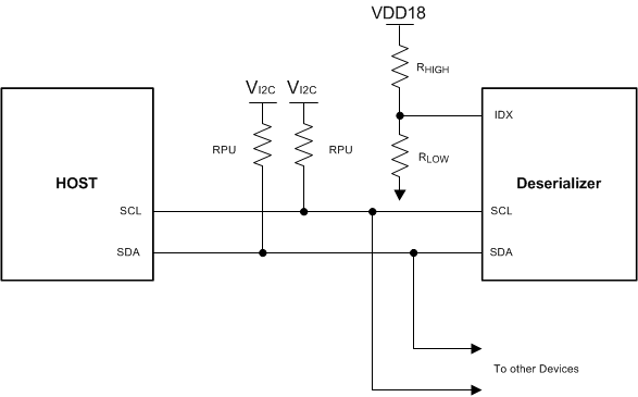
The device address is set through a resistor divider connected to the IDx pin (R1 and R2 – see Figure 7-19).
 Figure 7-19 Serial Control Bus Connection
The serial control bus consists of two signals, SCL and SDA. SCL is a Serial Bus Clock Input. SDA is the Serial Bus Data Input / Output signal. Both SCL and SDA signals require an external pullup resistor to VDDIO. For most applications, TI recommends a 4.7-kΩ pullup resistor to VDDIO. However, the pullup resistor value may be adjusted for capacitive loading and data rate requirements. The signals are either pulled High, or driven Low.
The IDX pin configures the control interface to one of eight possible device addresses. A pullup resistor and a pulldown resistor may be used to set the appropriate voltage ratio between the IDX input pin (VIDX) and V(VDD18), each ratio corresponding to a specific device address. See Table 7-15, Serial Control Bus Addresses for IDX.
| NO. | VIDX VOLTAGE RANGE | VIDX TARGET VOLTAGE | SUGGESTED STRAP RESISTORS (1% TOL) | PRIMARY ASSIGNED I2C ADDRESS | ||||
|---|---|---|---|---|---|---|---|---|
| VMIN | VTYP | VMAX | VDD18 = 1.80 V | RHIGH ( kΩ ) | RLOW ( kΩ ) | 7-BIT | 8-BIT | |
| 0 | 0 | 0 | 0.131 × V(VDD18) | 0 | OPEN | 10.0 | 0x30 | 0x60 |
| 1 | 0.179 × V(VDD18) | 0.213 × V(VDD18) | 0.247 × V(VDD18) | 0.374 | 88.7 | 23.2 | 0x32 | 0x64 |
| 2 | 0.296 × V(VDD18) | 0.330 × V(VDD18) | 0.362 × V(VDD18) | 0.582 | 75.0 | 35.7 | 0x34 | 0x68 |
| 3 | 0.412 × V(VDD18) | 0.443 × V(VDD18) | 0.474 × V(VDD18) | 0.792 | 71.5 | 56.2 | 0x36 | 0x6C |
| 4 | 0.525 × V(VDD18) | 0.559 × V(VDD18) | 0.592 × V(VDD18) | 0.995 | 78.7 | 97.6 | 0x38 | 0x70 |
| 5 | 0.642 × V(VDD18) | 0.673 × V(VDD18) | 0.704 × V(VDD18) | 1.202 | 39.2 | 78.7 | 0x3A | 0x74 |
| 6 | 0.761 × V(VDD18) | 0.792 × V(VDD18) | 0.823 × V(VDD18) | 1.420 | 25.5 | 95.3 | 0x3C | 0x78 |
| 7 | 0.876 × V(VDD18) | V(VDD18) | V(VDD18) | 1.8 | 10.0 | OPEN | 0x3D | 0x7A |
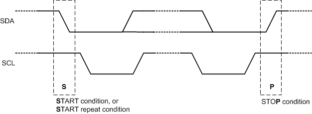
The Serial Bus protocol is controlled by START, START-Repeated, and STOP phases. A START occurs when SDA transitions Low while SCL is High. A STOP occurs when SDA transitions High while SCL is also HIGH. See Figure 7-20.
 Figure 7-20 START and STOP Conditions
To communicate with a remote device, the host controller (master) sends the slave address and listens for a response from the slave. This response is referred to as an acknowledge bit (ACK). If a slave on the bus is addressed correctly, it acknowledges (ACKs) the master by driving the SDA bus low. If the address does not match one of the slave addresses of the device, it not-acknowledges (NACKs) the master by letting SDA be pulled High. ACKs can also occur on the bus when data transmissions are in process. When the master is writing data, the slave ACKs after every data byte is successfully received. When the master is reading data, the master ACKs after every data byte is received to let the slave know it wants to receive another data byte. When the master wants to stop reading, it NACKs after the last data byte and creates a stop condition on the bus. All communication on the bus begins with either a Start condition or a Repeated Start condition. All communication on the bus ends with a Stop condition. A READ is shown in Figure 7-21 and a WRITE is shown in Figure 7-22.
 Figure 7-21 Serial Control Bus — READ
 Figure 7-22 Serial Control Bus — WRITE
 Figure 7-23 Basic Operation
The I2C Master located at the Deserializer must support I2C clock stretching. For more information on I2C interface requirements and throughput considerations, refer to I2C Communication Over FPD-Link III With Bidirectional Control Channel (SNLA131) and I2C over DS90UB913/4 FPD-Link III With Bidirectional Control Channel (SNLA222).